AM
modulation with solid state 2015
I wanted to make an AM modulator to modulate any sine wave
between 100kHz and 2MHz.
Googling will show a few schematics for RF signal generators but
virtually all search results do not have
enough information to build anything worthwhile. I hope my
schematics here give more understanding
for what could be useful workshop test gear.
The schematics here use discrete discrete solid state devices.
There is nothing here which uses factory
made function generator chips and 1,001 other supporting parts
or op-amps.
AM modulation continues to be widely used in electronics
since AM radio transmissions began by about 1920.
Methods here produce milli-watt level RF signals to simulate AM
radio transmissions for testing AM radios etc.
I wanted AM production with :-
1. AM carrier RF bandwidth 100kHz and 4MHz, -1dB, 65kHz
to 4.5MHz, -3dB, and NOT using any tuned LC networks.
2. Flat response of audio F modulated envelope between
10Hz and 20kHz, -3 dB poles.
3. Less than 3% THD in envelope shape at 97% mod using
1kHz audio sine wave with audio THD < 0.01% THD.
4. Envelope THD % declining linearly so at 50% mod, THD
< 1.5%, and negligible levels below 10% modulation.
5. Freedom from parasitic oscillations and spurious
noise.
6. The same modulated envelope for 97% modulation should
occur for a wide range of RF carrier input levels and for
a wide range of AF input levels between 10Hz and 20kHz all
without constantly adjusting audio input levels to get good
looking waves at 97% mod.
7. Ability for linearising the non linear modulation
process by local detection of AF to be used for NFB to reduce
envelope
shape THD.
8. Ability for use as peak voltage detector with or
without out AM modulation.
There are two input signals required to produce an
amplitude modulated signal, the input "carrier", Vc, and
modulating
signal, Vm.
The frequency of Vc is usually more than twice Vm. It is
possible to have Vc = 80Hz and Vm = 20Hz, and the
arrangement of devices will produce an 80Hz tone which varies in
amplitude at a rate of 20Hz. This idea has sometimes
been used in guitar amps with tremolo function where all AF
between say 40Hz and 8kHz can be varied in amplitude
at rates between 2Hz and 10Hz.
This page deals with Vc being RF over 100kHz and Vm is audio
signal between 5.0Hz and 20kHz or slightly higher.
The basic principle of producing AM is :-
1. Active devices are set up with fixed input low level input of
Vc, the carrier, in this case RF.
2. Vc carrier current change in active devices is low.
3. Vm, a modulating signal with different F to Fc is applied to
cause a higher change of current change in the active devices,
bjts, mosfets, j-fets, or vacuum tubes.
4. The modulating Vm signal causes device Gm to change
approximately linearly to applied Vm voltage, and the Gm can be
reduced to zero, or to about twice the idle Gm.
5. The change of Vc carrier current in devices = Vm x Gm. The
amplitude of the Vc current is thus changed between zero
and twice the idle value, and this gives maximum possible
amplitude modulation of carrier signal.
The basic process is the same for all Vc frequencies
including AF or RF and circuits may be similar, but C, L and R
values chosen may be very different for the range of frequencies
involved. This page explores the use of Vc <
100kHz
and change of current and Gm in mosfets and bjts at modulation F
between 5Hz and 20kHz.
The changes in currents of both LF modulating signal and HF fast
carrier signal produce signal voltages in any load
resistors which are used in series with drains or collectors.
The RL signal voltage in Vrms = Gain of device x input voltage.
The gain of devices with high internal drain or collector
resistance such as mosfets and bjts = Gm x RL, where
RL < R internal / 20. The voltage gain is also subject to
effect of device capacitances but we need to ignore C while
considering basic function at fairly low F.
Fig 1. VERY basic AM gene.
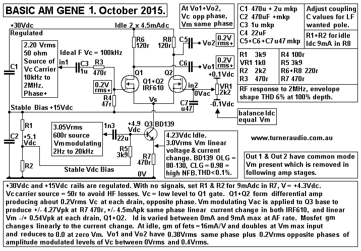
Fig 1 Vc carrier input F can be between 10kHz
and 2MHz, but here I found operation between 100kHz and
1MHz to be fair. When Vc has its amplitude varied linearly with
a lower F audio signal, the carrier "carries" the
audio wave information without the presence of the modulating
signal.
Where Vc > 100kHz, it is easily transmitted across air or
space as RF energy, and so much more efficiently
that shouting at each other over long distances or using
telegraph poles and wires, although fibre optic
cables and satellites do give relief to the mass of messages we
send!
The modulating signal is Vm, and here is considered
between 5Hz and 20kHz.
Carrier amplitude changes convey the volume change heard, and
the peaks and valleys of envelope shape
conveys the AF frequencies. The envelope shape for music &
speech shows constant complex carrier
envelope shape. But with Vm = ONE sine wave at ONE AF, we can
see the Vc envelope shape change
as a regular pattern on a CRO and we see that its outline
boundaries above and below the 0V axis have
the shape of 2 phases of Vm.
In Fig 1, input Vc = 100kHz = 2.2Vrms. It is reduced by
network C3+R3+R4 to 200mVrms and applied to
Q1 gate, and the signal supply resistance of at both Q1+Q2 gates
= 42r Q1+Q2 work as a simple long
tail pair differential amp which produces equal but oppositely
phased Vc signals at drains. Q1+Q2 sources
are commonly connected to a high ac impedance current source of
collector of Q3.
Each Q1+Q2 drain has same R load, and carrier Vg-s for Q1
and Q2 is same, but opposite phases
and thus balanced. Q1+Q2 act like any LTP, or differential amp
with high resistance current supply
to commoned sources, and with Vc input to only one gate, with
other gate grounded.
The Vc RF level needs to be kept low to minimize THD in
Vc. The small change in carrier RF current
during each carrier wave means mosfet Gm does not change much
during each small RF wave.
The change of current at modulation F is much higher so there is
a large change of Gm.
The idle current in each mosfet = 4.5mAdc, and this is moved
down to 0.0mA and up to a peak 9mA.
The change of current in both mosfets is the same, and has the
same phase at modulation F.
The change of current is achieved by connecting both Q1+Q2
sources to collector of Q3 which is a
"linear voltage controlled current source", with Vm audio input
voltage controlling current in both mosfets.
With no Vm input, only Vc signals are seen at each drain
and with no amplitude change.
Gm of each mosfet in class A with idle Idc = 4.5mA is 16mA/V, so
RF gain with RL 120r = 1.92,
so with 0.2Vrms gate to gate Vc input, Vc drain to drain =
0.384Vrms, or about 0.19Vrms at each
drain, and carrier current = 0.19V / 120r = 1.58mArms=
+/-2.23mApk, so just under 1/2 the idle
current in each mosfet.
Maximum Vm input is where Id is reduced from idle to
0.0mA, then to a maximum of twice
idle Id, ie, between 0.0mA and 9mA max. This aims to give 100%
AM modulation. You could
further increase Id, but high distortion of envelope occurs. Vm
input must be kept within practical
limits. With Vm current change of +/-4.5mApk, Vm signal voltage
change at each 120r = 0.0 to 1.08V
= +/- 0.54Vpk = 0.38Vrms.
Both Vm at both 120r have same phase and appear to have the same
wave shape of the audio
Vm input to Q3 base.
Without any Carrier Vc input, but with maximum Vm, only
Vm waves are seen at each drain.
But when Vc is applied to gates, you will see Vc appear at
drains in addition to a constant Vm.
There is a simple addition of two signals being added to a
simple load resistance. But you will notice
the HF Vc has much amplitude change and biggest Vc change is
when Vm has reached its maximum
peak level as I show in Fig 2 below.
If Vc input is held constant, and Vm increased above 0V,
and Vm and Vc levels are measured at
each
120r, the Vm amplitude change is accompanied by Vc amplitude
change of same magnitude, so the
applied Vm is linearly amplitude modulating the Vc.
The process is not perfectly linear. The shape of the
modulation envelope can have typical THD = 5%
at 100% modulation when envelope is on the brink of developing
flats on wave peaks, ie, clipping.
The envelope THD Where there is 5% THD in envelope shape, it
shows in compression of maximum AM
wave peaks, so Vc is being compressed and some 3H or 300kHz is
being produced. This distortion
of Vc is seen with a pure R drain load, but would be excluded if
drain loading was a tuned LC.
Keeping drain Vc just below 0.2Vrms at idle without
modulation gave carrier THD just low enough.
Audio F modulation Vm is applied to to Q3 base. Q3 has
high enough emitter load R7 470r so
that it operates as a linear emitter follower with THD in Vm
currents < 0.1% at highest wanted levels.
Q3 has far higher Gm than mosfets so its open loop gain is high
and local follower NFB ensures a
linear I change with Vm change. The Q3 emitter Re 470r ensures
collector resistance is a virtual
pure current source which is linearly controlled by Vm applied
to Q3 base.
Q1+Q2 commoned sources form a very non linear input
resistance load varying between very high
ohms at 0.0mA and 15.6r at Ic max 18mA. So the Vm waves at
both Q1+Q2 sources look very
distorted and like rectifier signals in a PSU.
Max Vm change at Q1+Q2 sources is about +0.8Vpk and - 0.2Vpk..
Fig 1 shows VR1 pot set up for slightly changing Vdc gate
bias to balance idle Idc in Q1+Q2.
This is important to prevent distortions and to equalize
amplitudes of outputs at each drain.
This simple AM modulator is not perfect. Some THD
of Vc and Vm is produced.
If Vm voltage content at each drain is removed entirely, the
"envelope" shape of the modulated Vc
waves may have about 6% THD at 97% modulation. The envelope
shape may have mainly 2H
with lower levels of higher H. The envelope THD % reduces at
lower levels of modulation
so is low at 10% modulation but rate of increase in THD is not
linear, and depends on unpredictable
transfer curves.
If Vc is transmitted with envelope distortion, an AM radio
receiver will reproduce all THD in
detected AF signal. Many old radios may add several % of THD and
IMD so it easy to hear
the shortcomings limitations of poorly modulated and transmitted
and received AM radio.
CRO 1. Views of AM Envelope shape distortion.
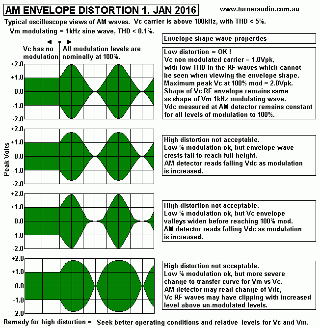
CRO 1 shows what range of possible distortion may be found
during construction of a SIMPLE AM modulator.
Most ppl who try to make an AM modulator to give less than 5%
envelope THD at 100% modulation will find it
very difficult because there are just too many things to get
just right, such as :-
Definition of mission plan, Device choice, Understanding of
basic device properties, Idle current in devices,
Resistance termination of device electrodes, Level of applied Vc
to input of current modulated devices
Level of applied Vm to modulating devices, Values of R, L and C.
All the distorted wave forms are a result of one or more things
which go not allow a linear change of device Gm
directly proportional to the applied modulating voltage. The
challenge is to overcome the problems to give envelope
THD less than 5% at 99% modulation.
COWPAT = 1 / N squared. This the Disgusting Formula
which applies itself to all aspects of our lives. :-)
Chance Of Working Perfectly Any Time = 1 / ( Number of things
you did not get right )
If there are 6 things, the COWPAT = 1/36, = 2.77%, so never kid
yourself that you are just like the Pope, and Infallible.
-----------------------------------------------------------------------------------------------------------------------
To properly test AM radios, an RF gene is used and should
produce AM waves to test the whole AM broadcast band
between 522kHz and 1,719kHz and the IF amp which may
need IF signals between 100kHz and 480kHz, with most
common IF = 455kHz.
I have not tried to make AM modulators for F above 2MHz, and I
found it much more difficult to get low envelope THD
at 2MHz than it is at 100kHz. Probably, the internal capacitance
for many SS devices prevents linear modulation as F rises.
If the AM detection in AM radios is found to have low THD at
very low signal levels which do not generate AGC voltage,
they may usually be found to sound OK when detecting short wave
bands between say 5MHz to 22MHz.
If IF amp and AF detector are found to work linearly, then the
alignment of SW band LC need only be for maximum
signals over widest spread of F, and to maintain tracking where
the difference between tuned RF input and local
oscillator Fo is the IF, usually 455kHz. Sadly, this is not
often the case in all AM radios, including many much loved
sets dating back to 1930. If the short wave RF is say 14.0MHz,
and RF input coil and FR amp output coil should both be
tuned to 14.0Mhz, and oscillator should be 14.455MHz. If the SW
band is from say 9MHz to 22MHz, getting all
3 tuned LC to be correctly tuned is not so easy, and where F is
say 5% away from correct F there may be high
in detected envelope. With an AM generator, one may view the
detected AF wave as the LC are tuned and usually
the AF is highest, generated AGC is highest, and envelope THD
lowest where every coil is tuned correctly, but
also where the AGC -Vdc is not at minimum or at maximum. There
is a sweet zone for best AM reception.
I repaired dozens of old AM radios and most gave very non hi-fi
performance.
The effort on this page is to explain AM modulation with
SS, and does not provide details for any tunable RF
oscillator, aka VFO.
It is easier said than done to make a good modulator as
an add-on unit with a handful of discrete devices and
which is usable with most simple stand alone RF and AF
generators.
Fig 2. Vc 455kHz + Vm 30.33kHz for Fig 1 schematic
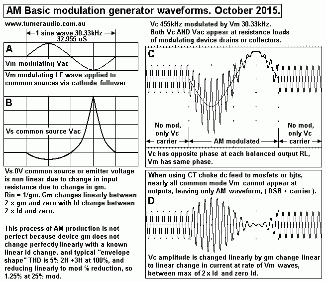
Fig 2 shows working wave shapes in schematic in Fig 1 :-
A = Vm input signal voltage to Q3, 30kHz.
B = Common source Vac at Fig 1 Q1+2 sources, and it is at
30kHz but with very high even numbered H
products because of large change of non linear source input
resistance.
C = Waves at ONE of the drain load resistors, say R6,
120r. At the other load R8 120r, the same wave seems
to appear, but only the Vm component is the same phase and
amplitude, while Vc has same change in amplitude
but it is of opposite phase.
D = Wave achieved at each drain load when Vm is removed
from signal by following device stages or by use of CT
choke with low resistance, or by use of transformer, which then
excludes the passage of any small amount of Vm
which may appear across the primary with CT.
The carrier = 455kHz and modulation is by 30.33kHz,
and modulation depth = 100%.
In the real world, in most signal generators, Vm of
30kHz or higher is never used because the highest audio F
= 20kHz, and highest AF for AM broadcasting < 10kHz, ie, all
AF < 9kHz, and anything above 9kHz is sharply
attenuated.
I have used 30kHz to make the waveform drawings more easily
understood with each individual carrier wave
seen fairly clearly. In the real world there is no pixilation
and you see smooth curves on the oscilloscope.
Fig 2-D shows the Vc AM wave without presence of Vm which
appears at each R6+R8. D shows a constant Vc
followed by Vc changing its amplitude so the positive Vc peaks
describe a sine wave of 30kHz. The negative Vc
peaks also describe a 30kHz sine wave, but produce an opposite
phase of 30kHz.
Vc at R6 and R8 = 0.2Vrms = 0.28Vpeak. I show Vm = 0.56Vpeak,
and total maximum Vpeak-peak of Vm + Vc
total = 0.56V + 1.12V = 1.68Vpk-pk. This peak-peak Vac change
across 120r produces 14mApk-pk.
This pk-pk current change = sum of Vm current change of 0.0 to
9mA peak plus Vc current change of 4.7mA
when Vc has doubled from the idle level.
Fig 2-B shows common source waves at Q1+Q2 sources. There
is high THD because the change of current
is from a virtual voltage controlled current generator Q3
collector, and the common sources of Q1+Q2 form a
resistance = 1 / ( 2 x Gm ) where Gm is transconductance of each
mosfet which varies during each Vm wave
cycle between 0mA/V and 16mA/V.
In other words, the input resistance looking into commoned
mosfet sources is highly non linear.
The Gm is approximately proportional to source / emitter
current, so Gm varies with Vm input to Q3, but the
action produces about 6% THD in envelope shape even when most
variables are optimized, showing the
process is far from being perfectly linear.
The waves in 2-C at each of Q1+Q2 drains look strange,
but comprise 2 simply mixed signals added together,
Vc + Vm, with amplitude of Vc varying because the Gm change
during each cycle of Vm and the Vm waves
appear linear because the current input change to the sources is
linear, with Vm current THD < 0.1%.
In practical circuits, the output from drains or
collectors with R loads at C are subjected to a LPF which
excludes the Vm content. The wanted HF Vc content remains
and is shown in wave D.
The LPF function can be achieved by using CT choke feed to Q1+Q2
drains or by a following differential
amp stage with high common mode rejection. Opposite phase
differential Vc is unaffected, but common
mode Vm is nearly eliminated.
Complete elimination of Vm is only possible with the
choke loading of modulator devices and as shown
in Fig 5 and Fig 6 below for the best SS AM generator I could
invent and with good common mode rejection of Vm.
Fig 3. Shows a 100% modulated Vc at 455kHz with Vm
30.33kHz.
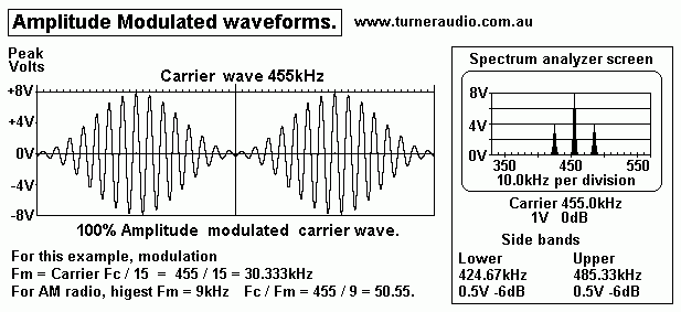
The spectrum analyzer shows there are 3 frequencies
present, lower side-band, LSB, Carrier, upper side-band, USB.
The analyzer would show four F present at each of Q1+Q2
drain outputs in Fig 1 because of presence of Vm.
Fig 4. Basic AM gene with choke feed of Idc to each
mosfet drain.
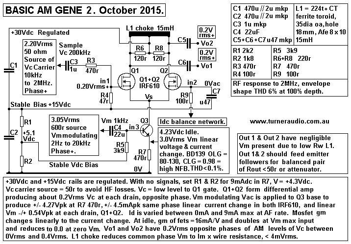
Fig 4 shows identical operation to schematic in Fig 1 -
but with the addition of L1, a toroidal cored choke with CT
to feed Idc to each mosfet Q1+Q2.
The common mode Vm signals
at drains is suppressed because the choke inductance couples
each half winding
magnetically and common mode voltage applied to each end of
choke create opposing magnetic fields, and current
cannot flow differentially.
However, some Vm current does flow across the choke where
current in Q1 and Q2 is not exactly equal, ie,
slightly unbalanced. Distortion currents related to Vm may
also appear where you don't want any.
XL1 15mH = 95r at 1kHz, high enough to allow
differential Vm signal to appear at drains but there is very
low
differential signal and some very low common mode Vm present
is generated in wire resistance of each 1/2 winding
of choke.
The 120r drain loads must be used to ensure there is a
fixed finite R load for Vc. Without 120r, differential Vc
output levels would vary hugely because of variation of
inductive reactance ohms for Vac applied. Without a low
value shunting 120r. L1 becomes a tuned LC with whatever self
C exists in the coil plus C looking into mosfet drains.
The Fo resonant F will be within the desired RF bandwidth, and
above this F the total shunt C reactance causes
reactive load value to reduce with higher F. To reduce effects
of reactive loading and resonances, the L1 is shunted
by resistance lower than XL or XC within the wanted bandwidth.
The modulator output resistance is determined by
120r, and the circuit is immune to outside loads of following
stages. With R = 120r, the C for a -3dB change of load
and gain drop at say 2MHz is 662pF, so that a following stage
of load of 220pF won't reduce Vc by -3dB until 6MHz.
In practice, getting to 6MHz with Fig 1 circuit is impossible
because of other internal shunt C in mosfets all working
together to stop you getting what you imagine might be
possible.
I found it impossible to get a nice looking envelope
shape at 100% modulation and at 2MHz, no matter what
changes I made to Vm and idle Idc and feed of Vc to gates.
Possibly the use of drain loads as low as 12r0 and
gate input loading of 5r6 may overcome C effects, but then
output drain signal levels would be 0.02Vrms instead
of 0.2Vrms, and wanted high Vo levels at output of unit would
be much lower.
L1 Core should be equal to that advertised by Jaycar,
material "type 15", It is Jaycar Cat No LO-1238, a toroid,
unpainted, dark grey. It has permeability µ at 20kHz above 10,
much higher than a ferrite rod. Jaycar also have
a slightly larger yellow painted toroid which has a lower µ so
don't use this. The grey LO-1238 needs less turns for
a given L than a rod or an air cored coil which must have much
larger dia and many more turns with higher wire
resistance and higher self capacitance.
I used about 2 Meters of Cat 5 with blue outer
sleeve removed, and wound about 28 turns of the 4 pairs
of
polythene insulated wires wires to fill the toroid hole fully.
The centre of the 2M wires were anchored with tape
at a starting point on core, then 1M each side of center was
easily threaded around through toroid hole until
one layer is achieved, about 14 turns. The other 14 turns are
wound over top of first 14 turns to give a total of
28t for each of 8 wires.
The 8 windings were connected in series on a small
adjoining terminal board. Measured L was about 15mH
at about 10kHz, XL = 942r, and at 100kHz it is at least 9k0,
so there is negligible inductive load at all F above
100kHz. If total R shunting L = 240r, the mosfets are loaded
only by R at wanted F for Vc. Shunt C in coil plus
shunt C between drain and source prevents response going as
high as I might like, so use of RL on each
side of choke could be as low as 33r, which will reduce Vc
output from 0.2Vrms to 0.055Vrms, a rather tiny signal,
but it probably would allow F extension to 4MHz.
The IRF610 are a popular RF power mosfet but they do
have fairly high internal capacitances so operation
with untuned L+C drain loads requires low R load values to
maximize HF bandwidth. You are free to experiment
with other mosfets to get better performance.
I found IRF610 gave higher envelope THD than BF469 bjts
which roughly equaled THD produced by a pair
of 6EJ7 pentodes with screen modulation.
Fig 5. BJTs used for AM modulator.....
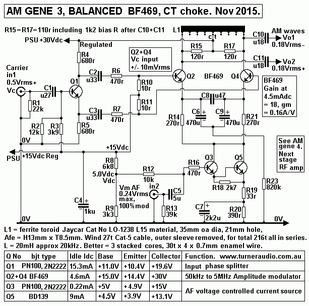
Fig 5 has Q1 as split load phase inverter feeding
balanced Vc input to Q2+Q4 bases. Q3+Q5 form a Darlington
follower for a voltage controlled current source to alter
emitter current of Q2+Q4.
The Vc input needed is much less for BF469 because the bjt gm
is 10 times higher than IRF610, and to
produce the same signal at collectors the base Vc signal may
be much lower. Q1 provides good HF
performance to 7MHz.
L1 choke with CT feeds Idc = 4.6mAdc to each Q2+Q4
collectors. The pair of BF469 were chosen from 20
samples to have hfe = 135 +/- 5%. R&C emitter bias
networks ensure Idc balance.
The linearity of Q3+Q5 as a follower deliberately
reduced slightly by using a low value of emitter resistance
R19,
only 33r. Only 0.22Vrms is required across R19 for current
change of +/- 9.2mApeak. The Q3+Q5 open loop gain
is less than 12, and the 2H generated is about 3% at max Vo.
This has opposite phase to envelope 2H so the
THD of Q3+Q5 is reduced about 1/2 by cancellation during
modulation.
R15+R17 Loads on Q2+Q4 collectors = 120r, and following stage
bias R = 1k2. The load values may have to
be reduced to give a total of 50r if that is the only way to
get a flat RF response to 5MHz.
Notice R23 820k which has no effect on signal function but
pulls the negative sides of C6+C9 towards 0V to
polarize the electro C properly.
------------------------------------------------------------------------------------------------------------------------
Examining envelope linearity.
There are several ways to check if modulation is linear.
1. The simplest way uses triangular Vm input wave at
1kHz, with and compare the Vm with Vc modulated
wave shape with a dual trace CRO. It is easy to overlay the Vm
on top edges of envelope shape and adjust
Vm to be equal to envelope shape between 0% up to 50%
modulation. The input Vm wave does not have to
be a perfect triangular wave shape because we only want to
know the difference in shape between the Vm
and Vc envelope shape. When modulation is increased beyond 50%
to 100%, the increase of envelope
shape should remain equal to Vm wave, but this seldom occurs
and envelope increase falls behind the
Vm wave by as much as 10% which is easily seen. The use of
sine wave Vm will also give the same result.
If envelope THD is under 2%, it becomes more difficult to see
in the CRO using this simple method.
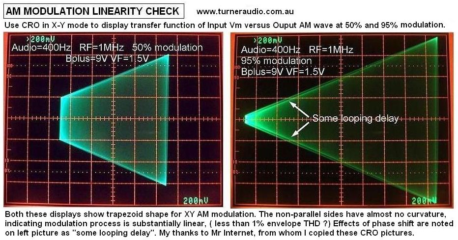
2. The other classic way to examine modulation
linearity is to use a CRO in X-Y mode with Vm vs Vc.
Vm is usually 400Hz, sine wave. Without any modulation, you
see vertical a straight line, but as modulation
is increased above 0% you see a trapezoid appear and at 100%
modulation the two sloping sides should
extend to a point leaving a green triangle with 3 nice
straight sides. The two sloped sides of trapezoid should
be straight, often the sides curve inward to the point of 100%
modulation which shows the Vc amplitude is
failing to remain linear to amplitude of Vm. But 1% distortion
may be difficult to see while 6%+ is very easily seen.
CRO 2. Views of Linearity check.
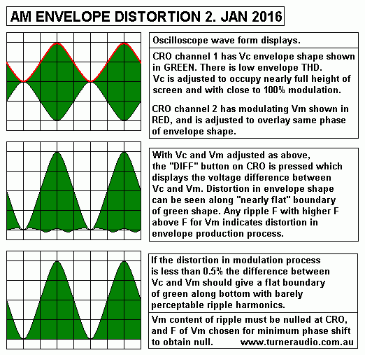
3. Another method uses dual trace display of envelope
and Vm with Vm overlaid on envelope at 100% mod as
mentioned in method 1 above. The envelope shape of Vc at 100%
is adjusted to occupy the full height of CRO
screen on channel 1, and Vm input wave occupies 1/2 height on
Channel 2.
In Dual channel mode, Vm is overlaid on top or bottom 1/2 of
envelope depending on phase of Vm. Then you press
the "add" button where the CRO adds the Vm to Vc or you can
press the "diff" button where CRO displays difference
between Vc and Vm. Either way you will see ONE modulated Vc
envelope for total height of screen, and a flat
boundary line at bottom or top of screen. This is the result
of simply mixing Vc with Vm.
Some CRO adjustment of Vm amplitude will remove slight ripples
in flat boundary of Vc. Some ripple in this line has
same F as the Vm, but cannot be fully reduced because of phase
difference between Vc envelope and input Vm.
Vm F can usually be changed between say 100Hz 2kHz to find F
where there is minimum phase shift and Vm riple
can be nulled fully. The remaining ripple in flat boundary of
Vc will be higher F than Vm, mostly 2H or 3H, which
is the THD in the envelope, but not in Vm. But when envelope
THD < 0.5% with fairly modulation at 100% mod,
the Vc flat boundary has imperceptible ripple.
When you examine a few AM modulators the linearity differences
become very easy to see.
The THD % = 100% x ( pk-pk ripple / pk-pk envelope shape. )
Relative pk=pk voltage levels are easily counted using the CRO
screen divisions. My Hitachi CRO has 8 main
divisions across and down, like a chess board with 64 squares,
and each side of square is divided into 5 "graticules" .
A typical result is flat boundary envelope ripple = 2
graticles pk-pk, total envelope = 40 graticles, so envelope
THD = 100% x 2 / 40 = 5%.
When THD is reduced below 1% at 97% modulation, you will have
trouble seeing it on the CRO, and you then have
done a fairly good job!
CRO 3. Views of AM Vc wave minus Vm modulation wave
4. The other method involves use of low THD Vm input
sine wave at say 1.0kHz. The Vc AM
wave is detected using a low THD envelope detector. Most
simple diode+C+R detectors can
get their THD down to 1% at 100% mod, so if you measure 2% THD
in detected AM at 97% mod
then you have about 1% of THD added by modulation process. It
is possible to make an envelope
detector giving much less THD, so that if Vm input THD =
0.001%, and detector THD = 0.1%, and
you measure 1%, then the modulation process is adding nearly
1% THD.
--------------------------------------------------------------------------------------------------
AM modulators are prone to additional oscillations
higher than Fc and appear as wave forms riding
on the carrier. When viewing envelope shapes of Vc waves on a
CRO, you may see bands of faint
changes of green intensity in displayed envelope shape. This
indicate the presence of unwanted
oscillations. When no spuriae are present, the green envelope
should have uniform green color.
Brightening of boundaries on envelope edges can mean the
carrier waves have compressed
appearance, ie, slight flattening of peaks, which indicates
generation of 3H. There is quite a lot to see
on a CRO if you know what to look for. A good radiologist will
see much more on an X-ray than you might
see.
--------------------------------------------------------------------------------------------------
Fig 6. RF amp, source follower output and choke,
switched attenuator.
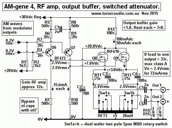
Fig 6 shows a balanced RF amp has gain of about 12x
using 2 x BF472, pnp, with local current FB
and low RL values and high idle current to keep RF response
flat to above 6MHz. This stage follows Fig 5
modulator schematic.
Output from Q6+Q7 collectors directly drive gates of Q8+Q9
IRF610 in source follower mode which drive
RFT1 ( auto-transformer ) with CT which gives 4 output taps
each side for 4 switched output levels.
RFT1 has 8 windings using 4 pairs of lightly twisted
wires from Cat-5 cable. It can be the same as described
above, but below Fig 4. The 8 windings are symmetrically in
series so connections of ends of windings form
output taps taken to a 2 pole x 4 pos rotary wafer switch to
give 4 levels of RF output.
Total voltage gain of Q6+Q7 and Q8+Q9 for 100kHz to
6MHz = approx 12x, so if input to Q6+Q7bases
Vb-b = 0.4Vrms then Vout across whole of L2 choke = 4.8Vrms.
Output resistance at each output for
highest Vo = 7r0. For switch positions giving lower Vo, Rout
reduces due to transformer impedance change.
I show Q8+Q9 = n-type IRF610 but BF469 should be just
as good, and with R11+R13 both 75r, idle Idc
will be 50mAdc each. Max theoretical Iac = +/-50mApk = 37mArms
in each Q8+Q9. If each Vo at each source
= 2.4Vrms at highest switch position, minimum balanced load =
130r, or 65r at both outputs, and for class A
operation. If Vo is drawn from one output only, lowest RL =
33r for 2.4Vrms. 175mW is available.
For the lowest switch position with Vo from one output side at
0.6Vrms, L2 TR = 4:1, ZR = 16:1, so balanced
load could be 8r0, or 4r0 from one output. RFT1 has good
magnetic coupling because all its 8 windings are
effectively multi-filar wound close and all magnetically
parallel to each other. Low loads below the standard
50r for a signal gene RF output can be tolerated.
----------------------------------------------------------------------------------------------------
It is remarkable that in 1950s HP achieved a good
result in their HP606A which had 6 well calibrated RF
ranges for 150kHz to 65MHz and good AM envelope shape with 2 x
6CL6 pentodes using a 6B4 triode for
cathode modulation. But they had exquisitely crafted coils and
4 gang tuning cap for the PP RF oscillator with
12AT7 and output tank circuit for 6CL6. Linearity was made
acceptable using DC and AC global NFB.
HP produced the HP606A with only tubes, then the HP606B with
solid state in PSU, but same RF and AF signal
circuitry as 6060A with tubes. It does seem possible all tubes
in HP606A could be replaced with solid state, but
you have an enormous amount of work to get all going as well
as HP could achieve.
Conclusions about solid state modulator.
The BF469 bjts in modulator stage worked better than mosfets
such as IRF610. But both device types produced
high THD ( over 5% ) in envelope shape at modulation > 95%
with carrier F above 1MHz.
I spent 2 weeks full time trying to optimize the
voltage and current settings, but I concluded these SS devices
did not work with untuned loads as well as vacuum tubes with
tuned loads for modulators.
I spent another 2 weeks trying to make a simple AF
detector to produce an AF signal with low THD during
detection.
This wasn't too difficult. The detector was to provide AF
signal for use as NFB applied to a simple wide band
differential amp so that envelope THD could be reduced from 6%
at 90% mod to less than 1%.
This seemed like such a simple idea which would work,
but I soon found I could not succeed because the smallest
application of NFB to correct envelope shape THD always gave
every possible type of parasitic oscillation and
some unusual inexplicable behaviour.
I then concluded that NFB probably was never ever going
to work because the modulator stage has very wide
bandwidth and gain for all F between 50kHz to 3MHz. The AF amp
could not rely on gain shelving and phase shift
reduction below 20Hz and above 10kHz to avoid parasitics,
similar to how stability in pure audio amps is achieved.
There seemed to always be an F where oscillation would occur,
or the CRO screen would fill with amplified noise.
The only way I think I could could avoid parasitic F
was to use tuned LC in collector circuits with Q at least 10,
so that high gain is confined to the tuned bandwidth of LC.
I wanted minimum RF to be 100kHz, not that far above
the audio band. This is a bit low for for LC, but I could have
I have tried using dual radio tuning gangs, with each gang
giving total C between 48pF to 480pF. These could be
arranged for 3 switched RF bands, 170kHz to 544kHz, and 530kHz
to 1.7MHz and 1.7MHz to 5.4MHz. 3 switched
coils with CT are needed, 3.8mH, 0.38mH, 0.038mH. The
complexity required with adding switched coils and
tuning C become extremely difficult to get working correctly
with equal Vo levels for each F along each band
and equal for all 3 bands.
Then the input RF signal has to come from a suitable RF
oscillator which should ideally have 3 switched RF bands
with identical F to modulator so good tracking must be
achieved. The RF output from RF oscillator must have a
fixed output level for all F between 170kHz and 5.4MHz, and
set for optimal operation. All this is ALREADY done
in a HP606A tubed RF gene which has 6 switched RF bands
between 150khz and 65MHz, all nicely calibrated.
It soon will become obvious that 3 switched RF bands to 5.4MHz
will not be easy with an ordinary 3 position rotary
switch wafer switch because of unwanted couplings and
oscillations. I have built enough RF genies to know this,
so its better to restore a HP606A or B than build your own
modulator.
A PP modulator stage is not essential. SE circuits can
work fairly well and this means all LC can be ordinary
unbalanced LC with one L and one tuning gang.
I concluded I could not succeed well enough with
solid state and untuned loads, and I changed direction to
re-building a tubed RF gene and modulator with SE oscillator,
and PP modulator needing the same single L in
oscillator and output amp and with a 3 gang tuning C.
-----------------------------------------------------------------------------------------------------
Fig 7.
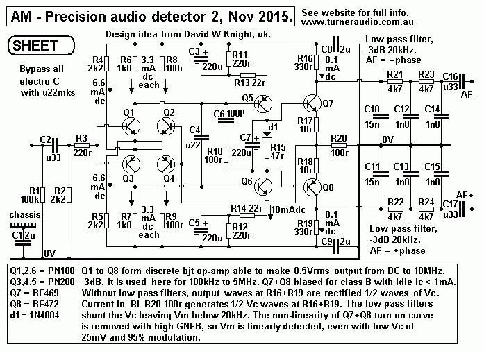
Fig 7 has an op-amp design I have used before for wide
bandwidth test gear. Its application here is based
on an idea mentioned by Mr David W Knight of UK in
his online published hand drawn schematics.
Fig 7 is quite simple compared to what would be found
in many IC op-amps. Unlike most IC op-amps,
TWO additional outputs are available from collector current
sensing resistors, apart from the usual single
terminal for signal output.
The op-amp is capable of 0.71Vrms input without THD up
to 5MHz. This is much better than many op-amps
which cannot be used above 200Hz.
When Vc carrier input = 0.707Vrms, and applied to +non
inverting input port of amp it produces about
0.702Vrms across load of R20 100r, a permanently connected RL.
The output to this load is all fed back
to input inverting port for NFB to make the amp work like a
normal op-amp in unity gain follower mode.
The load is a pure 100r, with no shunt C so amp is immune from
phase shift with outside world C reactance
loading. There is a critical damping Zobel network R10 100r +
C6 100p to ensure there are no parasitic HF
oscillations.
Now Q7+Q8 are biased for class B with Idle dc < 1mA.
The open loop voltage gain at say 1MHz is at least
100, and when 5mV input is applied, Q7 or Q8 base voltage
swings +/-0.5Vpk before any R20 load voltage
begins to appear. With more than 5mV input, the Vo at R20
begins to closely follow the input Vc increase, and
R20 load signal becomes linear to Vin because of the NFB loop.
So Vo is virtually equal to Vin, ie,
if Vin = 0.707Vrms, Vo = 0.702Vrms.
Thus the non linear turn on character of the bjts is corrected
by NFB, ie, the crossover THD in output load is
reduced to negligible levels. The bjt turn on curve is like a
silicon diode, and this non-linearity is avoided in the
output.
The current flow in R20 100r load is then linear to
Vin, and each 1/2 wave of carrier Vin generates linear
half wave currents in R16 + R19. If maximum Vrms across 100r =
0.702Vrms, Vpk = 1.0Vpk, so max current
= 10mApk. R16 & R19 are each 330r, so peak Vac = 3.3Vpk.
The Vac at R16 are half sine waves going negative
blow the B+ rail, and at R19 the 1/2 sine waves are positive
going from B- rail.
At 100% modulation, carrier Vc input changes between
0.0V and 2Vpk, so peak Vac across R16 + R19 vary
between 0.0V and 6.6Vpk. These 1/2 wave peaks can only be seen
clearly on a CRO when there is no C across
330r, and no following low pass RC filtering to remove carrier
half waves while allowing modulation waves to pass.
Now Q7 & Q8 have very high internal collector
resistance and they act like a voltage controlled current
sources
to feed Iac to the relatively very low value collector RL of
330r. So the equivalent circuit is a voltage generator
with series R = 20k approx feeding 330r. The effect of any
bypass C across 330r on bjt current production is negligible.
To see what is happening.........
Fig 8. Half wave average RF voltage detector.
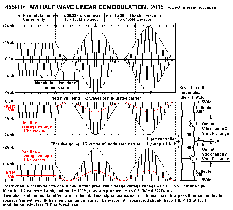
If collectors are shunted to 0V by a large value C, then no
Vac appears across 330r. But the ac current signal is
that of a 1/2 wave rectifier and there is a Vdc change across
330r which is the "average Vdc" level for 1/2 sine waves.
If the C is large enough, the change to average Vdc is slowed
right down and the Vdc remains constant regardless
of whether the modulation is anywhere between 0% and 100%. The
effect of shunting collector loads 330r has
zero effect on the working of the amp and makes no change to
the current change in bjts unless the amp is
driven by such a high level Vin that Vac across 100r + 330r
reduces Vc-e to less than a few volts, and devices
are saturated, because their effective Vdc between emitter and
collector limits voltage and current movement.
Normal operation here is well short of levels causing device
saturation or overload.
If we measure the Vdc across a large C across 330r, we will
Vdc across C = average Vdc = 0.315 x average
Vpeak Peak. At all levels of modulation %, the average carrier
peak Vac remains constant so that with or without any
C across 330r, a meter with high Z input will read Vdc
determined solely by carrier level. So in this case, average
Vdc across 330r varies between 0V when bjts has virtually zero
current, and 3.3Vpk for average peak carrier level.
Vdc across 330r = 0.315 x 3.3Vpk = 1.04Vdc. The same
sort of waves occur in 1/2 wave mains rectifier circuits.
If there was a full wave rectifier of sine waves, average Vdc
= 0.63 x average peak levels.
The constants of 0.315 or 0.63 apply only for pure sine
waves. The constants are lower for triangle waves and
0.5 and 1.0 for square waves. But where carrier input is most
often an RF sine wave with THD < 5%, average
voltage constants are correct "enough".
Now let us suppose we reduce the C value from a high
value to an intermediate value so that the RF half waves
are shunted, but lower F audio waves are passed. Fig 6 shows
C10 and C11 = 15nF shunting R16 and R19 330r.
The -3dB pole is 32kHz. What the CRO will show across each
330r is much reduced level of 455kHz 1/2 waves,
while 10kHz audio modulation waves will pass without much
attenuation. But it all looks like a horrible mess,
so additional RC filtering can be used with two cascaded RC
filters using 4k7+1n0 each giving poles at 34kHz.
The end result gives audio signal with bandwidth > 10kHz,
-3dB and very little 455khz ripple content.
There is no AF THD caused by diode forward voltage drop
and varying ripple voltage levels seen in ordinary
diode+C+R type of detectors. Such a detector works well with
Vc carrier input < 25mVrms.
You can expect that where you have you have 0.71Vrms
carrier input and 100% modulation, you should get two
opposite phased audio output signals each = 0.7Vrms.
In SS AM radio receivers the above
detector will work well; they may not generate IF signals
exceeding 1Vpk.
In tubed AM radios, IF signals can be between 4Vpk and
20Vpk from local stations and signals would overload
the Fig 7 schematic above.
For tube radio detectors see my detector schematic using
cathode follower to power diode+C+R detector
at Kitchen Radio.
----------------------------------------------------------------------------------------------
How to build stuff :-
Find huge amounts of time for stuff which may take
a year.
Prepare for Despair and Disappointment over poor initial
results.
To get good usable results, the following approach is required
:-
1. Learn by doing, build small schematics and work upwards.
2. Write down wanted F ranges and expected behavior during use,
compare ideas with other manufactured
test gear, get pencils, erasers, several 128page A4 exercise
books to draw all proposed ideas, and keep
drawing results and schematics and conclusions and test results,
every time you are at your bench.
3. Read old text books used by students at university for
electronics degrees in 1960.
4. Build a 1960 circuit, and wear out a pocket calculator
getting all R, C and L values right.
5. Get it working at one frequency.
6. Ask 101 questions about why it works and how it works, and
answer all questions.
7. Extend F range.
8. Possible help may come using Spice simulation software, but
guys in 1960 did have a brain inside head
and this isn't rocket science.
9. Eliminate shortcomings of each stage before proceeding to
next.
10. Apply whatever measures are needed for wanted correct
operation, ie, low THD across each F band,
flat output voltage across each F band.
11. Tidy up untidy circuitry.
12. Make dial plates, calibrate dials and label all knobs and
switched and terminals.
13. Draw up schematic with ALL details and print out copy to
always be placed inside metal box of the test
gear to allow instant service ease without searching forgotten
details you worked out 4 years before.
-------------------------------------------------------------------------------------------
To Education and DIY directory
To Index