Tubed
RF signal generator with AM and FM 2015
Towards the end of 2015, I decided to rebuild my RF signal
gene I first built before 1999.
It had 1/2 12AT7 for Hartley oscillator, see page 51, Fig
24.4B RDH4.
I had an SE pentode RF amp with 6EJ7 with tuned anode LC.
Grid modulation was used with
AF signal from 12AT7 diff amp which had AF input to one
grid, and GNFB to other grid from
diode+C+R detector of generated output AM wave. Envelope THD
at 90% modulation was reduced
from 7% to 1.5% with NFB. I wound the layered coils on short
lengths of ferrite rod, and I used a
2 gang radio tuning cap made in 1950s. Although useful, my
primitive effort left a lot to be desired.
The old circuit has been entirely revised and PSU was moved
from inside original metal box to a
second box attached at the rear, which gave me more space to
fit everything on Sheets 1, 2, 3
below. I now have these features :-
VC1 = 3 gang tuning cap driven with 3.5:1 vernier reduction
drive, each gang allowing total C change
= 40pF to 500pF approx.
VC2 = Small tuning gang for fine F adjustment of oscillator
to accurately settle F on a wanted nominal F.
S1. F range selection with 1950s re-cycled ceramic 4
position rotary wafer switch for :-
1. FM selection.
2. 525kHz to 1.75MHz, with ability for 100% AM modulation.
3. 375kHz to 520kHz, with ability for 100% AM modulation.
S2. FM nominal centre F selection, 4 position rotary wafer
switch :-
1. FM off, ( AM on. )
2. 455kHz, +/- 40kHz variation.
2. 745kHz, +/- 30kHz variation.
3. 1,200kHz, +/- 30kHz.
S3. 11 position rotary switch for RF output attenuator, for
-6dB steps from
1.2Vrms down to 1.2mVrms, ie, from 0.0dB to -60dB.
BNC jack 1. Output terminal for single phase AM RF band
signals with Rout 33r,
for all S3 positions, 1.2Vrms down to 1.2mVrms.
BNC jack 2. Output terminal for 0.16Vrms single phase FM or
0.4Vrms non modulated RF, Rout = 90r.
RCA jack 1. AF input terminal to input VR1 to set level
modulation %. 2.2Vrms AF input for 100% AM.
RCA jack 2. Output terminal to monitor AF after VR1, or
monitor sample of ramp signal after VR3,
with both for XY mode on CRO.
S4. 1 pole x 2 position for choice of AF input or saw-tooth
ramp level at RCA 2.
VR1. AF input level control.
VR2. FM centre Fo adjust.
VR3. Ramp level control to alter FM F deviation to max of
+/- 40kHz.
S5. On-off mains switch with LED.
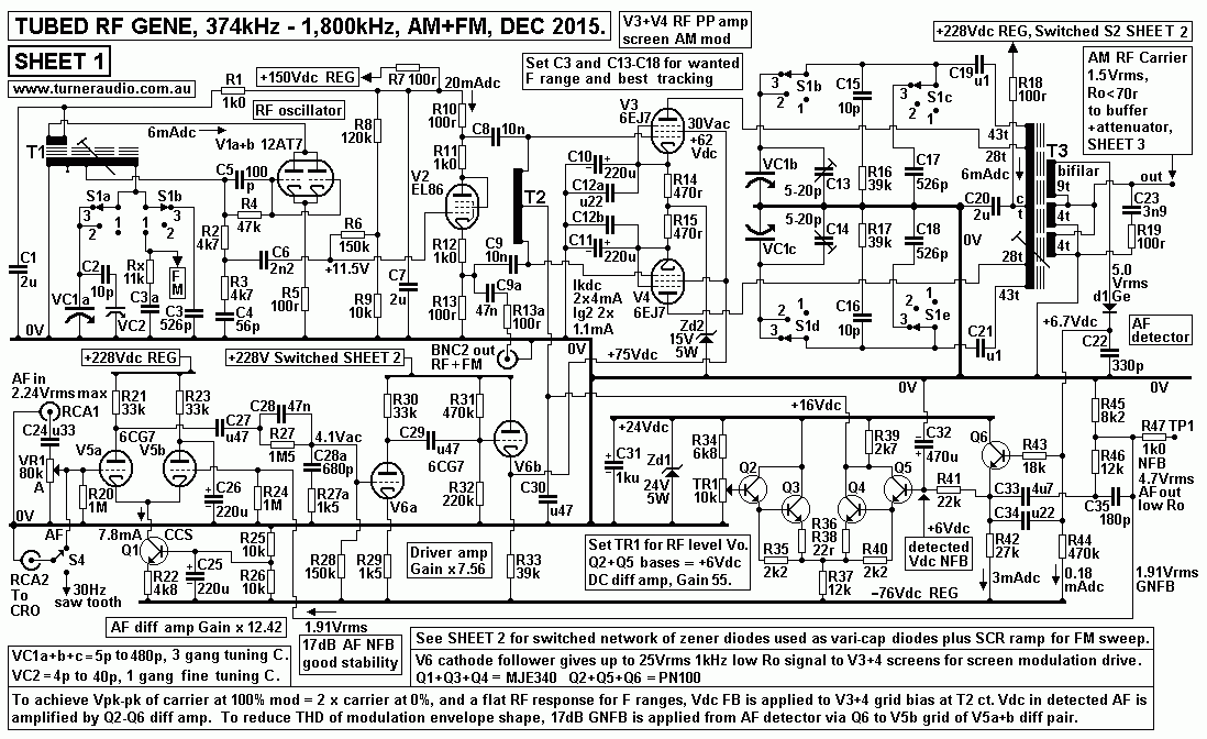
Details of RF gene are on 4 sheets.
SHEET 1, RF oscillator, buffer, RF amp, AF amp with NFB and
for AM screen modulation.
SHEET 2, FM generation and switched B+ for AM and FM rails.
SHEET 3, Output buffer amp and output attenuator S3.
Schematics are all .gif, B&W only, and may appear too
small in some browsers. But each schematic
can be enlarged to to better fill a PC screen for better
viewing, and can be printed to fill a single A4 page.
Fig 1. SHEET 1. Most of the the tubed RF and
modulator schematic.
All the above Sheet 1 plus content of Sheets 2 & 3 below
are fitted on a re-cycled zinc plated steel chassis
from an old AM radio, about 320mm wide x 190mm deep x 55mm
high. I've added 1.6mm AL front plate and
perforated zinc plated sheet metal for sides and back to
make box 190mm high.
There are 2 x PTs in PSU and mounted in additional steel box
320mm long x 190mm high x 100mm x deep
attached to rear of box for RF and AF circuits. There are a
large number of electrolytic filter caps from
my collection of spares, and a good number of high wattage R
for RC filtering.
The larger PT has 12.6Vac rectified for +16vdc, reduced by
RC to +12.6Vdc for all tube heaters except
EL86.
HT winding on large PT is 200Vac to make +265Vdc, RC
filtered before solid state regulation for
B+ and B- rails = +228Vdc, +150Vdc, -75Vdc.
The smaller PT generates +/- 16Vdc, RC filtered to +/- 14Vdc
for solid state buffer with 1RF610.
A doubler produces +32V, RC filtered to 24V, shunt
regulated.
PSU is not shown because anyone building this needs to be
able to design and build their own to suit
transformers and other parts are available to suit the
signal circuitry as I show. Any variations to
rail voltages will require serious changes to signal
circuitry.
Top cover of box is 1mm steel plate, raised 7mm above four
sides to gain a ventilation gap for outgoing
warm air. The box lid hole 120mm x 100mm centered above the
vertical oscillator coil. This prevents the
reduction of coil inductance and increase of Fo when lid is
fixed. The whole lid has non-metallic fibre
board covering.
All circuitry is point to point with tag strips and
different colours of insulated stranded wire.
There are a few small boards for some solid state circuitry.
Whole unit has 2 wood strips 16mm high x 25mm wide running
front to back on bottom plate
to allow air flow under and up through well perforated
bottom plate. Chassis plate has many
more drilled holes than it had originally, all to prevent
everything getting hot without needing a fan.
RF oscillator is a classic tuned grid oscillator using
single ended parallel 12AT7, needing 6mAdc.
T1 is wound on 100mm long ferrite rod for two switched RF
bands, 375kHz to 520kHz,
and 525kHz to 1,750kHz. One gang of 3 in a 1960s nicely made
radio tuning cap is used for the
high RF band, and for low band, 526pF is switched across the
single tuning gang.
T1 is slightly unlike anything else you'll find....
Fig 2. Ferrite core coil for tuned grid oscillator.
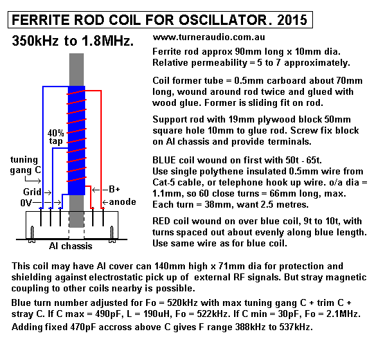
I did not need an electrostatic shield around the coil. For
those wanting to copy shielding practice
used in many old radios, they could use an AL can with
closed top, 140mm high, and 60mm minimum dia,
or square area 60mm x 60mm.
RDH4 has a lot to say about the effect of shield cans using
non magnetic metal, Al or Cu, on pages 438 to
441. DO NOT use steel sheet metal for coil shield of the
size I show.
The use of a steel case for the whole instrument is OK
because the steel is far enough away from coil.
With lid off box, and when Fo tuned for 533kHz, fixing any
lid, Fe or Al to box sides raised the tuned F
from 533kHz to 540kHz, and would disturb the tracking needed
between oscillator LC Fo and output
amp LC Fo. The ferrite rod end is only 18mm below sides of
box and the closer the lid, the bigger the
reduction of L. My solution to not having quite enough space
was a 100mm x 120mm hole in metal cover
pate, and the whole plate then covered with 6mm builder's
fibro. It is unlikely the opening in the box will
allow much spurious signal entry from other gear. Anyone
making anything like this needs to realize that
bench tests of coil inductance away from unit will give
different results when coil is mounted inside the unit.
In the past I have used shield cans sometimes taken from my
junk boxes. All of them changed inductance
when assembled over coil. I have found cutting a vertical
gap in can sides does reduce the effect of L
change because shield cans act like a slightly remote
shorted turn, as do a metal box with a lid.
The can is an effective electrostatic shield to prevent
spurious electrostatic coupling or RF pick up,
but there is little magnetic shielding.
To adjust L, the coil former position on rod must be
slightly movable. It can be fixed in position with dob
of silicone.
T1 needs to be well away from T3; I have T1 vertical and T3
horizontal and 200mm away.
The stray magnetic coupling is very low, and no cause for
instability. The layout prevents oscillator
signal entry into output buffer-attenuator which could make
it impossible to get 100% modulation.
Notice there are 10 turns for anode and spread along all the
turns for grid coil. This gave good
coupling between the two windings and there were no
parasitic oscillations which I found would
occur using any other arrangements and recommended in old
text books.
The grid is fed from a 40% tap on BLUE coil. The V1 12AT7
oscillator output level is controlled
by the grid current charging up C5 100pF discharged by R4
47k. The effect gently limits the anode
current so output is mainly only the tuned Fo.
The grid feed to V1 is from 40% of turns of L, effectively
from a source of 0.16 x tuned Z of the whole coil.
This means input C to 12AT7 grid does not affect tuning of
LC, or grid current affect the Q.
To ensure high Q of LC, and a wide range of tunable Fo, the
40% tap is a necessity.
The oscillator output does not give a flat response and I
found 6dB change across whole wanted F range.
The tuned impedance alters with F. I wanted a flat response
output and low Z, hence the other reason
for tap at 40%. This feeds an RC equalizing network R2+R3+C4
to give a flat F response between
375kHz and 1.8MHz, within +/- 1dB.
At 40% tap, max signal = about 15Vrms, with about 38Vrms
across the whole tuned LC.
The equalized output from eq network is about 4.8Vrms to
grid input of V2 EL86.
V2 EL86 is in triode, with healthy idle Iadc = 20mA and
works in concertina phase inverter circuit
with RLa = RLk = 1k1. Both 1k1 are 1k0+100r in series to
divide the +/- output down to 0.4Vrms
to drive output V3+V4 grids with a balanced signal at low Z.
V2 is a buffer stage creating
balanced sources = 90r. These drive ends of T2 choke.
T2 = 4.7mH choke with CT, wound on a 35mm toroid with µ = 15
at 1MHz, with 56 turns of 1 pair
of wires taken from Cat-5 cable. The two wires are connected
in series to give 112 turns total, with
56t each side of CT, and both 56t windings are bifilar, and
well coupled with fairly low self C.
Live ends of T2 couple to EL86 stage via 10nF and the
arrangement eliminates any differential
LF applied to output RF amp grids.
The RF output amp with V3+V4 uses 6EJ7 because I have a lot
of them, and they work well
enough for this application.
HP6060A has 2 x 6CL6, and these would have been better, but
harder to source. I could have
used EL86 or EL84, but probably with quite different idle
currents and other biasing voltages.
2 x 6EJ7 have Idle Ia = approx 3mAdc in each. Static bias
current is kept constant by a grid bias
Vdc controlled by a solid state differential amp and Vdc
feedback from the detected carrier
level.
I did consider anode modulation which could be done in this
application. But it would require screens
connected to anodes, and the whole output LC then has AF
voltage present. The use of triode may
give rise to spurious parasitic RF oscillations which would
need "neutralization" measures which
can be seen in schematics for "plate modulated" transmitter
circuits. With screen modulation,
the screens work to minimize C between anode and grid at RF
and I did not see any instability
which may have required ever more networks to gain
stability.
Fig 3. Ferrite cored balanced output coil for 2 x
6EJ7.
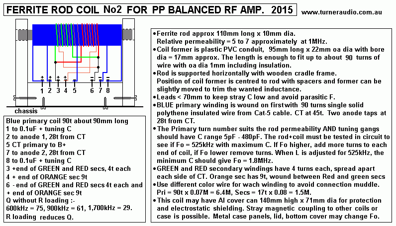
Notice the BLUE coil has taps 28t each side of CT for anode
so that the whole winding is not
loaded by effects of tubes which tend to reduce the Q and
limit the range of tuned F.
V3+V4 output tubes have screen modulation. Eg2 is supplied
from the fairly stable +75Vdc
output of V6b cathode follower which also supplies a maximum
of 30Vrms AF. V6b cathode
follower Rout < 500r.
Notice both screens are commoned, and the AF applied to
screens alters both Ia in V3+V4.
The change of Ia at AF causes a change of tube gm which
roughly linear to applied Vg2.
Thus the RF gain of the 2 x 6EJ7 is changed between nil and
twice the value at 100% modulation.
The process is far from perfect, and during each positive
going wave of AF the screen current
increases and anode dc current reduces which limits the
maximum levels of output RF.
To compensate the screens' robbing of Ia, the Ia is
maintained at the idle level by the increased
by DC diff amp of Q2,Q3,Q4,Q5.
Correct operation requires that detected Vdc from output
remains constant regardless of
the level of modulation. The DC diff amp has a reference
signal input from TR1 10k, and a
DC FB signal from AF detector of diode+C22+R44 which feeds
buffer Q6 emitter follower
The AF screen signal is produced by the differential amp
V5a+b and gain amp V6a+b,
using 2 x 6CG7. Overall gain is about 90x.
For 100% AM modulation, AF input = 2.24Vrms to V5a grid and
and there is 1.91Vrms of
NFB applied to V5b grid. There is 17dB of applied GNFB.
The AF signal for NFB is derived from AF detector of
diode+C22+R44 which feeds buffer
Q6 emitter follower. Emitter output is divided by R45+R46
with Vdc blocked by C33+34.
I have slight gain+phase shift compensation networks in AF
amp with V5+V6 and there
is excellent stability. If modulation input = 1kHz square
wave, there is virtually no overshoot
of AM envelope waves and no peaking of sine wave modulation.
(( This is a much better
outcome than in my original RF gene and much better than
produced by HP606A RF gene.))
With the GNFB, envelope shape THD < 0.8% at 95%
modulation, with a 6dB margin of stability.
RF output levels remain within +/- 0.5dB for the whole
wanted F range, regardless of
modulation levels.
With 95% modulation with Vm 400Hz the bandwidth for
envelope THD > 1% is from 10Hz
to 4kHz.
With 50% mod the non-distorted BW is from 8Hz to 15kHz. THD
reduces for lower mod levels.
If you examine most transmitted AM radio signals which have
little compression applied, the
average modulation level > 30%. THD of this unit <
0.2% at 30% mod, and definitely less than
any HD created in most old radio detectors with with
primitive tube diode +C+R all driven from
output from sec of IFT2.
The oscillator and RF amp MUST remain tuned to the same Fo
within a tolerance of +/- 4kHz
when tuning across each RF band. This isn't easy to achieve;
but we MUST have good tracking,
and not made any easier because oscillator coil and output
coils are of different design with the
only common feature being a similar ferrite rod.
The coils for T1 oscillator and T3 output can be wound to
details above and tested on the bench
to assess the basic properties when used with VC1, without
being in the unit box. A signal gen
with variable unmodulated Fo is used with 1k0 in series with
the untuned low turn windings.
The signal level at 1k0 connection to coils is monitored at
CRO and with F meter.
With VC1 fully meshed, you should get F range from 521kHz to
above 1,900kHz with VC1 fully
opened. If you get from say 600kHz to 2,200kHz, and with
coils at centre of rod, you need more
L and more turns. So add more turns until you can get 521kHz
to 1,900kHz. The rod length I used
just over 90mm, and the rod you may use could have different
"magnetic permeability factor", µ,
and there is no way anyone can assume they will get the same
inductance with different rods.
There is nothing to be gained by a longer ferrite rod, sa5
150mm+ because you'll have trouble
fitting it close to tubes and switches. I shorter rod could
be used, but then turns need to be
increased which increases coil self capacitance which
reduces the available F range.
The 100mm rod length is ideal, and allows coil turns to be a
single layer solenoid.
When you are confident you have the approximate turns
correct, you must terminate wire ends
with narrow strips or masking tape to stop turns springing
off from former and ending up a mess.
The wound coils should be painted with varnish. Clear
polyurethane furniture varnish is fine, and
you need a small 250ml can, plus a 6mm artist brush and
turps for clean up; I have used a strip
of cloth wound around a strip for a brush, and gasoline for
clean also OK.
The varnish will have a slight effect to increase coil self
capacitance. The coil self C is usually
less than 7pF.
A handy formula for RF coils is :-
C in pF = 25.35 x 1,000,000 / ( F kHz squared x L mH )
A typical oscillator coil L = 0.185mH.
The C required for 521kHz = 25.35 x 1,000,000 / ( 521 x 521
x 0.185 ) = 505pF
For 1,900kHz, C = 38pF.
The coil self C must be kept low to be able to get low
enough minimum C for the top end of
the tuned band.
The well insulated solid wire on ferrite core does give high
enough Q and bandwidth results
with low enough self C, and without needing litz wire which
can be difficult to obtain, and
difficult to solder.
To align this unit, discipline wins, guesswork leads
straight to failure.
Alignment is done with coils fixed to unit, assembly
completed and circuits wired
and able to work with DC. ( be prepared to re-arrange
layouts, do things twice of 3 times
before getting to work at least as well as I have managed ).
The oscillator Fo ranges are set first, and for broadcast
band of 521kHz to 1.75MHz.
The 3 tuning gangs VC1a,b,c are about 480pF max VC2 is
10-40pF small tuning gang for fine
adjustment of oscillator Fo once a nominal value has been
set.
T1 alignment.
1. With VC1 fully meshed, and VC2 at 1/2 rotation, T1 tuned
grid coil turns are reduced or
increased until Fo = 521kHz, with coil set at 1/3 of rod
length.
Secure loose wires at end of winding after turn adjustment.
Varnish coil a second time, but make
sure varnish does not leak to between coil former or rod
which will prevent fine adjustment of
coil position on rod.
2. With minimum turns set, further fine L adjustment is
possible by moving coil on rod; towards
centre = more L, towards rod end = less L, and coil former
may be secured with dob of silicone.
This will set hard in a day, but is easily removed with
knife for later L adjustment.
3. VC2 is opened maximally, and you are lucky if you get
maximum Fo = 1,900kHz, with VC2
in mid position. If you get say 1,600kHz, the minimum C is
too high, and your coil may have
too much self C, or the minimum C of tuning gang is too
high, or there's too much stray C in your
wiring method / layout.
With no tuning gang connected, you might get Fo = 2,200kHz,
indicating coil C plus any other C =
28pF. 1,600kHz indicates total C = 53pF, if the L = 0.185mH,
( 185uH ).
So you need a tuning gang which has low minimum C when fully
open, and lots of C when fully
closed, ie, with high C max / min ratio = 2:1, which allows
a low value trimmer C to be added to
set the HF end of the tuned band.
The wanted Fo max / min ratio is 1750 / 521 = 3.35, and C
max / min ratio is always the Fo ratio
squared, so 11.22 in this case.
I obtained this Fo ratio with minimum coil turns and minimum
C of coil. My layout with short leads
to / from switch has low enough minimum C and the tuning
gang has max C of about 480pF per
gang, and minimum C approx 20pF.
Some old tuning gangs have 350pF max, 40pF min, so coil
turns are high, and with other inevitable
stray C you may find you could only get 550kHz to 1,600kHz.
By 1955, there some very good tuning gangs made.
Tuning gangs for solid state radios were often only 160pF
max to 10pF min, so inductance would
have to be 9 times higher needing a ferrite rod coil with
2.25 times more turns. Millions of cheap
SS portable AM radios used 2 gang tuning C with very thin
but rugged plastic sheet between
sliding plates, less than 25 x 25 x 15mm These are not
suitable for this application.
3. The F range Sw1 is moved to low range. VC1 is fully
opened with VC2 in mid position.
The value of fixed C3 across L must be carefully chosen so
that Fo = approx 520kHz.
I used a polystyrene 470pF plus added 56pF to give highest
Fo for low range = 518kHz.
4. With VC1 fully meshed, I got Fo = 375kHz.This range
covers the IF used in most AM radio sets
except a few early AM sets before WW2 which had IF = 230kHz,
or some communications sets
which had IF = 100kHz. My unit here suits most AM radios
made after WW2. I do have other
oscillators for unmodulated signals between 2Hz and 2MHz
which can be used.
5. To adjust turns and L of output T3 LC, the Vdc NFB
circuit should be disabled by connecting
T2 CT to a fixed +16Vdc. This allows measurement of
uncorrected +Vdc produced by detecting
Vdc from carrier levels at T3 secondary, always using a
non-modulated RF signal.
T3 alignment.
6. With Sw1 set for broadcast band, and VC1 fully meshed,
and oscillator Fo = 521kHz, and T3
coil former near centre of rod, turns are adjusted for
maximum +Vdc reading at detected output.
The adjustment of turns on each side of CT on tuned winding
must result with same total turns
each side.
Following turn adjustment, the T3 coil former can be
slightly moved on rod for fine tuning.
7. With VC1 fully open, the oscillator Fo should be
1,750kHz, and you should need to add 5-20pF
trim C across each of two tuning gangs to give same HF as
oscillator. Trimmers may be single turn
ceramics, see C13+C14, across VC1b+VC1c, both set to mid
position for say 12pF.
With added C13+14, the maximum of VC1b+c increases slightly,
and reduces the T3 Fo slightly
which may require coil to be moved a tiny amount away from
center of rod to be able tune down to
521kHz.
The 1,750kHz end of band should be able to be tuned easily
with C13+14 for maximum Vdc
output with VC1 fully open.
8. When the oscillator Fo is altered to say 800kHz of
1,300kHz, you should see similar levels of
detected Vdc. If you tune right across both RF bands, a
graph drawn of Fo vs Vdc should vary more
than +/- 1dB.
The tracking can be very good, and just as good as I have
found in HP606A which has a much more
complex arrangement of coils and trim caps.
The alignment process should be repeated several times.
Performance with modulation.
The Vdc NFB circuit is allowed to operate. Select broadcast
band range and lowest Fo = 521kHz.
Without modulation, TR1 is adjusted for +16Vdc at CT of T2.
Using Vm = 400Hz, increase modulation to 95%. The AM wave
envelope should show little THD,
and you should get a rise of +1 to +2Vdc at T2 CT. As
mentioned before, anode Idc reduces with
increasing screen Vac change. Without the Vdc NFB the
detected Vdc of carrier will reduce a volt
and envelope will clip at perhaps 15% lower level than
wanted. With 100% mod, the total carrier
maximum Vpk-pk should be twice the carrier pk-pk without
modulation.
The AM wave envelope shape should not change for any
selected RF between 375kHz and
1,750kHz. If the envelope becomes distorted before reaching
full maximum, it is usually due to T3
tuning not following T1 oscillator tuning Fo. Perhaps you
will spend days to get all this working just
right.
The output LC circuit has added R+C Zobel networks loading
the 1/2 primary windings, 38k +10pF.
At lowest F of 375kHz, reactance of 10pF = 42k, so ZR+C =
56k approx. But at 1,750kHz, XC = 9k0,
and ZR+C = 39k, and the effect of Zobel is to increase R
load across tuned LC to flatten the response
of output stage. The T3 Q will slightly reduce, and make
tuning and trimming at HF easier, and to help
prevent parasitic Fo > 1,750kHz. The added R loading
makes it all work better. I found I needed to
add a Zobel 100r + 3n9 across the two paralleled secondary
windings of 4t each.
T3 has three sec windings. There are 2 paralleled 4t
windings produce Vc = 1.4Vrms with Rout < 70r.
This output drives a source follower buffer amp on Sheet 3.
It would be possible to use the two parallel windings in
series, for 2.8Vrms, and at max mod % the
max Vc = 5.6Vrms, or +/- 8Vpeak which is a little too close
to limits of low THD operation of output
buffer amp.
The third T3 secondary = 9t spaced between the two pair of
4t windings. This makes about 3.3Vrms
and is in series with 1.4Vrms for a total of nearly
5.0Vrms with Rout < 350r, low enough to drive the
diode+C+R detector network. The higher Vac obtained for AF
detection ensures the diode distortion
during detection is a small % of total THD at all mod %.
HP606A uses a triode-pentode 6AW8 for diff amp to drive 6B4
to give cathode modulation.
The diff amp applies both Vac and Vdc NFB correction to 6B4.
I found having Vac diff amp with GNFB
worked well with a separate DC diff amp which could use a
few small bjts which were not reliably
available in 1955.
Fig 4. SHEET 2, FM generated with zener diodes for
vari-caps.
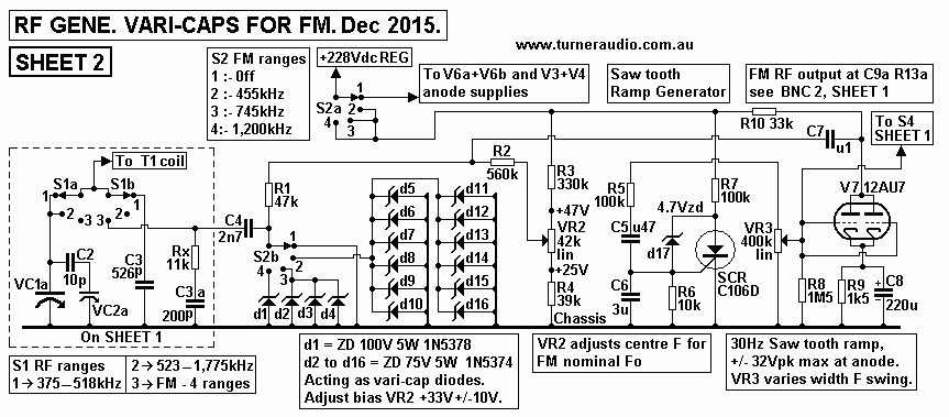
AM modulation is only possible with 2 positions of S1, AND
when S2 is switched to FM Off.
The third position of S1 selects FM.
With S1 selection of FM, Rx+C3a Zobel network is switched
across T1 tuned LC to reduce
the oscillator level to 4.4Vrms which applied to zener
diodes d1 to d16.
FM is only possible when S2 is switched away from FM Off.
Three FM ranges can be chosen.
With S2 in pos 1, FM Off position, B+ to V3+V4+V6 is turned
on to allow AM ranges, and B+
to SCR and V7 for FM is turned off.
This fiddly arrangement prevents the use of FM generation
during use of AM generation when
the saw tooth waves at SCR can cause 30Hz switching noise to
modulate AM.
All tube heaters operate continuously.
For 455kHz FM, S2 switches the oscillator coil to 12 x 75V x
5W, IN5374 zener diodes in parallel.
All the zener diodes in Sheet 2 work as vari-cap diodes able
to work with fairly high peak voltages
generated by the tubed V1 oscillator.
The Idle Vdc of 1N5374 should be just below 1/2 the nominal
zener voltage of 75V.
For all FM Fo ranges, the bias for nominal center Fo is at
+32Vdc, but able to be varied +/- 10Vdc
by VR2.
Each 1N5374 at +32Vdc idle bias has C = 53pF, with 49pF at
+43Vdc, and 57pF at +23Vdc.
For 455kHz, 12 x Vzd are used, for 745kHz, 3 x Vzd, and for
1,200kHz I have 1 x 1N5378,
with zener voltage = 100V.
VR2 allows the center Fo to be varied :-
455kHz range = 438kHz to 475kHz,
745kHz range = 708kHz to 775kHz,
1,200kHz range = 1,150kHz to 1,235kHz.
While the Vdc bias to zener diodes sets the centre Fo for
FM, a 30Hz saw tooth ramp signal from C106D
can be applied to V7 12AU7 grids to vary zener bias by up to
+/- 30Vpk. The FM frequency deviation is
approximately linear to the saw tooth voltage and deviation
range is controlled by VR3 400k. A sample
of the applied saw tooth ramp wave can be monitored with CRO
via S4 CRA 2 on Sheet 1.
The amount of F dynamic F deviation with saw tooth is more
than can be obtained by bias setting VR2.
The +/-30Vdc peak Vac applied to zener diodes is easily
generated by V7 12AU7.
The total Vpk-pk for RF and 30Hz saw tooth should not exceed
the zener voltage, in this case 75V.
Clipping of RF or saw tooth waves can occur if too much
total Vac is present. As I have it, the maximum
F deviation possible is obtained, and RF Vpk-pk = 12.3V, and
Saw tooth Vpk-pk = 60V, and total = 72.3Vpk-pk.
For highest FM Fo, I have 1 x 100V zener diode which works
well enough.
Zobel C3a 200pF plus Rx 11k. does not prevent V1
oscillating, but does reduce RF input to about 4.4Vrms,
quite enough level.
The FM generated by V1 working with T1 is fed through eq
network R2+R3+C4 and to V2 EL86 grid.
The FM level at V2 grid is about 2Vrms. FM output is taken
from R13 100r in V2 cathode circuit and then
to C9a 47n + R13a 100r. Level = 0.16Vrms, with Rout =
90r. This level is enough for most testing purposes;
if higher level of about 1.7Vrms is needed, C9a could be fed
from V2 cathode, where Rout > 150r.
The FM from V2 buffer is not passed through the RF amp
output stage because it is not needed very often,
and it is already modulated, and the switching complexity is
not necessary.
Attenuation of the FM signal must be done with external
attenuator, or use of variable wire antenna so an
AM receiver can receive the FM.
The arrangement allows a wide range range of FM to look at
the response of IFT amp or cascaded
RFT in AM radio sets.
The FM allows IFT alignment while watching pass band
response on CRO. The shape of the pass
band can be made ideally flat topped, important where IFT1
has its two LC adjusted for slightly
above & below the IF. Incorrect alignment or double
peaked response is easily seen using XY mode
on CRO.
There is no calibration markers for F but these are not
needed. The IF pass band response shape
can be plotted as a graph using small Fo changes of RF gene
without AM modulation and using a
digital F meter to plot a curve, and without receiver AGC
voltage applied.
In more complex equipment, markers for frequency during F
sweeps appear like pulses along the
band being observed, at say 4kHz intervals so that the
bandwidth is easily read from the CRO.
I have never seen a schematic for a marker "pip" but
probably a multi-vibrator circuit could be
arranged to produce a pulse after 4,000 cycle intervals of
any other F.
There is no room for such a "technician's luxury" in my
unit.
Fig 5. SHEET 3. Output buffer and Resistance
Attenuator.
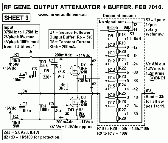
Low level output from secondary of RF T3 has source
impedance 70r and easily drives gate
of Q7 IRF610 (RF mosfet) in source follower mode with Q8 as
constant current sink = 200mA.
The PSU for this stage has +/-16Vdc from a 24Vac winding
with CT. The two rails have RC
filtering R1&2 10r0, C1+C2 10kuF for low enough ripple
+/- 14Vdc rails.
There was no need to regulate these Vdc rails.
Input Z to mosfets is high and the fairly low gate input C
loading has no effect on operation of
V3+V4. Output resistance from Q1 source < 10r0. Bandwidth
F1 pole is determined by C6 and
R8 33r. With S3 at pos 11 = 0dB and output load = 1r0,
highest F1 = 48Hz and F2 pole = 5MHz.
The attenuator S3 uses a re-cycled one pole x 12 position
rotary wafer switch with 12 terminals
with one terminal being the switch pole. This style of
switch allows 11 switch positions in this
application.
All R used for the switch except R8 are 100r 1/4 W, metal
film.
R9 to R17 are each 100r with R18 to R28 being 2 x 100r
paralled for 50r. This uncommon
arrangement for an attenuator gives equal output resistance
of 33r for all 11 output levels.
The levels are changed in -6dB steps, and if the output load
was 33r, then all levels would
reduce -6dB, and if RL was 16r5, all levels will change by
-10dB.
It is impossible to damage Q7+Q8 or attenuator if the output
is shorted. Without output loading
Vo = 1.2Vrms down to 1.2mVrms, -60dB. Lower level signals
are obtainable with additional
external attenuator. An antenna can be connected to
broadcast AM within a workshop for
pick up by AM receiver.
Back to DIY education
Back to Index