Wien Bridge Oscillator. August
2013.
This page describes a switched frequency Wien Bridge oscillator
with
j-fet Vo stabilization, buffered Rout = 55r, peak Vo max = +/-
5.1V for
both sine waves and square waves, switched attenuator for 4 levels
at
10dB steps below 0dB, and with logarithmic variable Vo. There are
6
ranges between 1Hz and 1MHz, with an F decade each.
There are 4 images,
Fig 1. Sheet 1, basic block diagram schematic of WB
oscillator with
details of switches.
Fig 2. Sheet 2, full schematic details of discrete bjt amp
for oscillator,
and attenuators, and buffer output stage.
Fig 3. Explanatory diagram of basic Wien Bridge network
with two equal
value R and two equal value C.
Fig 4. Schematic of Schmitt Trigger sine to square wave
converter with
2 discrete bjts.
I was cleaning up my workshop when I discovered I had been given
an old
BWD Electronics 141A audio oscillator which had many problems.
I delayed my life for 2 weeks while I rebuilt the darn thing.
It was made in Australia in the 1960s or 70s and designed to be
used with
batteries if need be.
Therefore it contained the bare minimum of current needing devices
and
used the bare minimum of other parts. Current and parts cost
money, and
bean-counters and CEOs hate any expenses, and BWD had no ambitions
to seriously compete with other expensive brands like HP at the
time.
The 141A unit was "budget test gear" and since it offered nothing
special,
it is not disrespectful to dismiss ideas used by the original
designers and to
consider the unit to be completely expendable in pursuit of better
operation,
while keeping the box, and the few parts inside worth actually
re-cycling.
I have never ever needed battery operated test gear, except my
DMM.
The only way to improve the performance was to revise the circuit
inside the
small box completely.
After measuring and making an intelligent appraisal of the
existing usability,
and having to give the unit a 1 out of 10 score, I removed all
discrete bjt + R + C
and tracks from the circuit board, except 6 pairs of plastic and
styrene C and
tracks around the interactive press button F range switches.
The 15k wire wound reverse log dual gang Compton pot for varying
was
intermittent and thus faulty and junked. It is impossible to
dismantle it and clean
it, or inspect its internals.
Switched resistors were used instead of a pot for F control.
I removed the entire PSU which was not original, but a replacement
installed by
a company 'Bodgy & Dumb P/L'.
The new PT and R+C parts of PSU are in a box screwed to the steel
plate
rear panel.
I put in a new amp on an additional board for the Wien bridge
oscillator.
Another board has the j-fet as variable NFB resistance needed to
control
output level.
I built a new Schmitt Trigger square wave circuit where the old
one was.
Another small board with a complementary pair of darlington
connected bjts
connected as a PP emitter follower buffer preserves the HF content
of all
output signals and reduces Rout to 55 ohms for all levels of
operation.
I re-designed the output attenuator switch to give 0dB, -10dB,
-20dB -30dB
levels which is more usable to me than the original. I replaced
the variable
output level pot.
My new circuits contain more parts than the overly simplistic
previous original
had, but it work better, and there is now no DC offset at the
output, and peak
voltage for sine waves and square waves is 5.1V, and the rise time
for square
waves excellent, 104V/uS. There still a few trim-pots to adjust,
and 3 trim C but
that is inevitable with much analog test gear where best
performance depends
on very small changes to R and C values.
There are 3 schematics :-
Fig 1 shows the switched R+C for C positive FB network and
the simplified amp
schematic with output attenuator and the negative FB network with
j-fet to vary
the amount of NFB.
Fig 2 shows the full details of the amp using discrete
j-fets and bjts which
gave wider BW than most common op-amps.
Fig 3 Gives basic properties of the Wien Bridge network.
Fig 4 shows the Schmitt Trigger square wave schematic.
Fig 1.
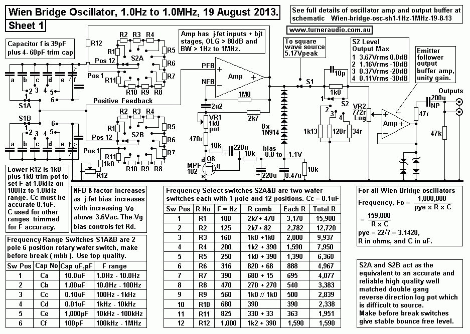
The Fig 1 schematic took me many hours to design and construct and
test and
adjust and revise before I got flawless operation over the six F
ranges covering
1Hz to 1MHz . The original BWD 141A Comptom pot was replaced with
a 1950
dual wafer 12 position break-before-make ( BBM ) switch
taken from a defunct tube
tester I was given which was quite beyond repair.
I found the amplitude bounced badly at first with this switch so I
converted it to
make-before-break ( MBB ). It required careful metal work
with 2mm x 3mm brass
plates and a steady hand with soldering iron and Dremel to clean
up where needed,
with two pairs of reading glasses.
This reduced the trace bounce on the oscilloscope.
If you build this, RS components sell suitable 40mm dia wafer type
switches with
MBB with 12 positions and 1 pole per wafer. I arranged the
resistance combinations
"R comb" hanging off the large lugs of the old rugged switch.
Although I show rotary switches for capacitors the original press
button spring loaded
interactive switches have been retained and the action is so fast
that little trace bounce
occurs from high transient amp voltages at amp Vo.
The much more detailed schematic of the oscillator amp, buffered
output etc and PSU is here :-
Fig 2.
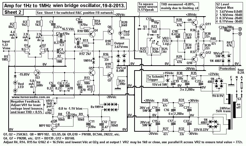
The original BWD 141A used an ITT P54 thermistor which is a low
wattage type
of 50k cold R and minimum of maybe100r. It was used where the Vo
was 2.5Vrms,
and thus 1.66Vrms was across the thermistor and this slightly
heated it to reduce its
resistance to approximately 2,000r. It worked well except that the
Vo bounced crazily.
It was used where the R12 2k7 above is used between oscillator amp
Vo and NFB
input port.
The principle with P54 is that If Vo rises, thermistor gets
hotter, reduces its R, and
increases NFB thus reducing Vo until an equilibrium is achieved
after the yo-yo of
Vo settles down. THD was at least less than 0.1%.
I didn't want to rely on getting a replacement P54 in future. No
modern thermistors
seem designed to work to give a sufficient temperature rise to
cause enough useful
resistance change. All mainly seem designed to change their
resistance usefully as
a result of an external change in temperature. So modern
thermistors are useless as
substitutes for P54.
In the case of the Wien bridge oscillator, we want the thermistor
( or lamp globe )
to operate at a near constant T well above room T and to vary its
R due to minute
changes to power and heat generated by Vac or Vdc across the
"element" or tiny
glass coated thermistor or tungsten lamp filament within a glass
tube.
But lamps are very prone to Vo bounce when switching anything,
because like
thermistors, some transient high current causes a delayed rise in
or fall or resistance
because temp change is not instant. Therefore, with temperature
dependent R
there is an unwanted time constant that can cause LF amplitude
modulation of
the Vo signal.
So, I changed the NFB circuit to use a j-fet and rectifier circuit
to produce a
negative gate bias of between about -0.8V and -1.1V.
The negative bias voltage for j-fet gate begins to be generated
when Vo = exceeds
3.2V peak. The 8 x 1N914 do not begin conducting until their
forward voltage = 0.4V
each, or 3.2V across all. The turn on voltage of a silicon diode
is not linear, and the
forward voltage across an Si diode does not reach a max of about
0.7V until the max
allowable rated I flows.
The series diode action was found to be a smoother than trying to
use a low voltage
zener and series 1 x 1N914.
When gate bias = 0Vdc, the j-fet has minimum Rd = 180r approx.
This then makes ß a lot less than 0.333 so that much less FB is
present and
oscillations start and increase Vo very quickly. But as Vo
increase, gate bias becomes
more negative and j-fet Rd increases which increases ß so the NFB
increases thus
preventing an increase in Vo when the NFB applied to Q2 gate is
very nearly the
same amplitude to PFB signal at Q1 gate.
Equilibrium is reached and oscillations and "magically", you get
the same Vo amplitude
for all F between 1Hz and 1MHz. The j-fet characteristic curves do
not describe their
properties fully but for each value of negative gate bias the
"diode" resistance line with
high line slope near vertical id axis varies with gate bias
voltage. What isn't shown is
that the Rd operates even if the applied voltage at drain goes
negative below the
source voltage.
The amount of current change in Rd across the Rd "diode
resistance" has to be kept
small because the diode R line on curves is not straight, and
rolls over to a virtually
flat high value R line because above about 2Vds, the Rd maybe
thousands of ohms.
If we have Vo at 3.66Vac, then there is about 1.22Vac at both NFB
and PFB ports of
the amp.
In fact, the amp has open loop gain at 1kHz = 40,000 approx, and
PFB voltage is only
0.09mV above the NFB voltage. The gate to gate voltage cannot
easily be measured.
The ideal region of operation for j-fet is where Rd = 300r approx.
If I have R12 = 2,700r,
and ß = 0.33, then the whole lower R of the FB network must be 1/2
x 2,700r = 1,350r.
The total R of both R = 1.35k + 2k7 = 4.05k, and if Vo = 3.66V,
then Iac = 0.903mA.
Therefore if Rd = 300r, then Vd = 0.271Vac, not much you may say,
but little things
have great and fundamental importance.
Therefore the VR1 1k pot plus R6 470r must equal 1,350r - 300r =
880r so pot is set
for 880r - 470r = 410r.
Because the R+C values used in the Wien network cannot be accurate
enough to
demand ß always exactly equal 0.33, and because of other slight
variables in the
circuit, using a pot for NFB adjustment is imperative.
If Vo goes higher than 3.66Vac, ß would rise above 0.333, and
oscillations would stop.
To gain equilibrium and thus Vo there must the pot VR1 1k0 to give
some fine adjustment of NFB so that oscillations do not dither and
bounce, or have
too much THD. The VR1 pot controls Vo across a small Vo range. If
pot resistance
is set high, oscillations to stop and start and "dither about",
but THD is low. If pot R
is too low then you get very stable Vo but high THD, easily
exceeding 3% mainly 2H
and seen in the CRO as you twiddle the trim pot with a screw
driver.
Between the two extremes there is a sweet spot where action is
good, and
THD < 0.5%, and the production level of gate bias with
diodes must be just right
to get the sweet spot.
To further reduce bouncing of the Vo level when switches are used,
the Vo has a
voltage clamp using 5.1 zener diodes and 1N4007 seen in Fig 2
below.
During switching, the oscillations try to change momentarily to
higher voltage
transient bursts of other F and as square waves.
The zener+diode clamp stops Vo exceeding about 5.7V which is
enough to prevent
most Vo bounce. The amp I have uses +/-20V rails and transient Vo
peak V can be
up to +/- 12V.
The circuit must not generate excessive gate bias quickly which
then subsides
much too slowly to allow oscillations to continue. All operations
MUST be free of
delays due to troubles with signal bounce and intermittent
oscillations, or delays
between stopped and re-starting.
The major troubles you never see mentioned or quantified in 99% of
online
information about Wien Bridge oscillators are the issues of
stability when changing F,
and the distortion generated by the darn little j-fet.
Now if you look closely to my above Fig 2 you will see I have a
local shunt NFB
network used between drain and gate using R8, C8, R9.
At above 1Hz, the ß = 0.5, and so 1/2 of whatever Vd exists is
applied to the gate,
so any THD generated by the j-fet is half applied to the gate,
thus it tends to be
amplified to reduce itself. Now the circuit works without R8, C8,
R9, and typical
THD will be 2%, mainly 2H, because the naked Rd without NFB is not
a linear
resistance but one which generates up to 10% 2H right at the
drain.
Part of this feeds into the NFB port and makes the maybe 2% of 2H
at Vo.
Now you may think the use of R8, C8, R9 changes the ß but they
make negligible
difference to the range of values wanted for Rd because that range
is between
about 200r and 1k0, and the loading effect is negligible. The R8
and R9 are 10k
each, and at very low F where C11, C12 are high Z, the value of
R17 needs to be
about 10k to prevent excessive FB at LF which makes LF stability
very bad because
you have a high open loop gain amp also involved and, where
possible, shit happens
that you cannot forecast. I had R12 = 100k at first and LF
stability was terrible, but all
calmed down when I made R12 = 10k. But then you need to have
sufficiently long time
constants for oscillation down to 1Hz so C11 had to be 220uF and
C8, also needed to
be 220uF.
The other needed thing about the NFB loop is that it controls the
amp Vdc output offset.
Ideally, Vdc at Vo should = 0.0Vdc, and pigs will fly before you
get that. BUT, I have used
fets for the amp inputs which have high Z in and thus I get away
with using the
C4 2u2 + R7 1M0 network to allow Vo DC to reach Q2g, without being
mauled by the
rest of the NFB network. The loading effect of 1M in parallel with
R12 2k7 is negligible.
With R8, C8, R9, the THD drops to less than 0.03%. But other
factors affect THD.
The limiting voltage clamp diodes begin to conduct on both + and -
wave crests at
Vo when Vo reaches +/- 4.9Vpk.
Such wave crest suppression causes some slight 3H++ to be
generated. But in my unit
I ended up getting THD = 0.09% at 1kHz, mainly 3H. This is much
better than having
2% 2H, and is much better than many other signal generators and
function generators
using chips to generate a fabricated sine wave.
I also tried 6 x series 1N914 in 2 directions ( 12 diodes total )
to act as a voltage clamp
plus VR pot across R12 2k7 but the sharp threshold action of
diodes causes high 3H
at maybe 5%, so that idea is hopeless.
I tried using a few 12V x 50mA lamps in series and a variable DC
current bias with pnp
bjt from +20Vdc. This made what I thought could be a good variable
R for NFB control.
Two more bjts and a rectifier were needed and it looked good in
theory but amplitude
stability was appallingly bad, so I quit that idea. THD was about
the same as the j-fet
with local FB though.
Now do you see how much everybody else online in the world does
not say about their
published electronic junk?
There is always more than ONE simple thing to consider about any
single R, C,
or any point of connection anywhere around any analog circuit.
But at least we can get an idea, something you cannot do with a
multi-layered PCB
with zillions of multi-pin ICs, all operating digitally.
The Fig 2 shows the whole voltage amp and it looks like a good
quality solid state
audio power amp. Indeed it could be a power amp but the load to be
driven is a
much higher ohm value so small signal bjts can be used throughout
and with
no heat sinks.
There are 4 loads on the amp, in parallel.
1. There is the NFB R network of R10, VR1, R6, and Rd of
j-fet.
2. There is the output attenuator, minimum 772 ohms.
3. There is the PFB network of switched R+C.
4. There is the series resistance R1 5k6 Fig 4 from amp to
Schmitt trigger square
wave circuit.
1. The NFB resistance network is always 1.5 x R12 = 1.5 x
2k7 = 4,050r.
Why? Because when Vo is stable and 3.66Vac, Q2 gate has 1/3 of Vo
present,
or 1.22Vrms. So there is 2.44V across 2k7, and I = 0.904mA so load
= Vo / I = 3.66 / 0.904
= 4.05k.
The PFB signal at Q1 gate may be 1.221Vrms and is only just above
Q2 gate.
The gate to gate voltage is extremely low where open loop amp gain
may be say
40,000 which would make Vg-g = 0.09mV, and quite difficult to
measure.
2. The output attenuator load is VR2, 772r and it came from
my junk box, and
seemed to have no serious faults so common in old pots caused by
dust, dirt,
pollution, corrosion, loose terminals, intermittent tracks.
I always clean out the pot with white spirits and plenty of
turning actions then blow
out with compressed air and then compress rivets holding lugs to
tracks using long
nose pliers in a vice. I seal up the hole near the lugs with
cardboard and tape and
THEN such pots give many more years of trouble free operation.
Most cheap log pots you buy won't be exactly 1k0, and somewhere
between 700r
and 1k2, and mine is 772r.
If I ever change to another "1k0" replacement LOG pot, a parallel
trimming R will
be needed to ensure the total nominal R value = 772r. If the R is
not 772r, the switch
S2 attenuator with its set resistances cannot give correct -10dB
reductions of output
signal amplitude because the attenuator R values are calculated
for only 772r.
-10dB is a nicely convenient reduction of output level. It means
Vo is reduced by
factor 1 / square root 10, or x 0.3162. This is near 1/3. Two such
reductions of x 0.3162
give a reduction of x 0.1, and you will eventually find this
engineers' way of reducing
outputs and inputs is a pleasure to use.
3. The positive
FB circuit is the Wien bridge RC network. For where the WB
network has equal two value C and R, the input load impedance
becomes
2.121 x resistance value, and because R is varied between R for
highest F
and 10xR for lowest F, the load we need to consider is the lowest
because
it needs the highest current and in this case R = 1,590r, and load
= 2.121 x 1,590
= becomes 3,372r. So where did the constant 2.121 come from?
The factor 2.121 is the factor calculated from 1.414 x 1.5. Huh?
Why?
In all Wien R+C bridges with two equal R and two equal C, the
output signal
response is that of a low Q tuned circuit and Vo can only ever
rise to 0.333 x Vin
which occurs at only one frequency, that of "resonance" Fo, where
phase shift
between Vin and Vo = zero degrees. See Fig 3 below.
Fig 3.
From the above basic Wien bridge when operating at Fo we see Vin =
10Vrms and
V0 = 3.3V. So that 6.67V exists across R1 in series with C1. And
we need to know that
phase shift between Vin and Vo = 0 degrees, lest all our
statements about measured
voltages are wrong.
At 1kHz Fo, reactance XC = R ohms, and impedance, Z for R and C in
series
= 1.414 x R = 2,248 ohms. Therefore current flow = 6.67V / 2,484r
= 2.966mA.
Therefore impedance looking into the input = 10V / 2.966mA = 3,370
ohms.
The result validity depends on the the 0 degrees of phase shift
between Vi and Vo.
The same 2.966mA flows through the Z of R2 and C2 in parallel, and
may be calculated
as 0.707 x R = 1,124r, or we may calculate from observations, Z =
3.3V / 2.966mA = 1,123r.
So total Z between Input and 0V = 2,248r + 1,123r = 3,371r.
The simplest way to calculate Z in for Wien bridge network at Fo
is Z in = 2.121 x R.
For decreasing frequencies below Fo, the Z in rises towards
infinity at 0.0Hz
because the C become open circuits.
For F increasing above Fo, Z in reduces to a minimum of R,
because the C become short
circuits at HF.
4. There is a
feed resistance from oscillator amp and square wave circuit, Fig
4, R1, 5k6.
The voltage at the Q9 base end of R1 is less than 1/5 of
Oscillator output so in fact
effective loading is about 6k2 from this resistance of 5k6.
( See how there is always more
than ONE thing to consider about any single part in
an electronic circuit! ).
So, we have 4 loads in parallel = 4,050r // 772r // 3,371r //
6,200r = 501r.
The amp must be able to power the load with little THD caused by
loading.
I like my signal generators to make +/-5V peak at least, and in
this case 3.66Vrms.
So load current at 3.66V = 3.66V / 501r = 7.3mArms. It could
easily be possible to
have idle DC current in Q6 and Q7 to give pure class A
operation if Ic = 11mAdc.
But this is not necessary, and the Q6+Q7 may operate in class AB
at low enough
THD because the NFB acts to reduce distortion in the amp which has
very wide
open loop bandwidth at 3.66Vac thus allowing 1MHz without any
attenuation.
But anyone is free to have Idc = say 20mAdc, and perhaps give
better HF stability.
I found that capacitive loads on the amp may cause oscillations
cease but very little
open loop HF gain reduction was needed with Zobel R+C between
Q4 base and Q4 collector, see R11and VC1, Fig2.
The Vo from the sine wave oscillator in Fig 2 is prone to poor HF
performance
especially if there is even a small amount of C, say 100pF between
the output side of
R16, 33r, and 0V. This is enough to cause phase shift and HF
oscillations above 300kHz.
But the shown switched attenuator S2 and pot VR2 cause negligible
C shunting
themselves. To protect the oscillator amp from effects of C
shunting of signal due to
cables or C in of gear and from low Rin of gear connected, I
decided a buffer output
stage was needed.
For a rugged buffer with wide bandwidth,
I used npn PN100+BD139 and pnp PN200+BD140 connected as a
complementary
emitter follower pair which gives gain close to 1.0. Its Rout is
set by 22r emitter resistors
and the 47r output resistance. A zener diode + diode 10V clamp
prevents high V from
something external to the unit providing a high voltage signal
back into the unit output
which would instantly fuse the bjts. The 47r is 1/8 W rated, and
fuses open if high voltage
enters the unit. Diode clamps are also placed from 22r junction to
rails for further
limiting of stray unwanted back flows of current, like when you
accidentally touch an
RCA lead on an anode at +400Vdc.
The buffer works in class A with all loads with Z above about
400r. Now that allows 400pF
as a load at 1MHz.
Class AB action occurs with lower loads. A shorted output with
maximum Vo of 3.6Vac
being generated causes a peak current of 74mA, and heats the 47r,
but won't blow it, and
causes about 0.5W of heat in each of BD139, BD140 which won't kill
them. Notice the R36,
R37, both 680r emitter resistors for drivers Q9 and Q10. These R
make the idle current in
Q9 and Q10 larger than if it was only the base current of Q11 and
Q12, and give a path for
discharging turn off current from bjts at HF, something bjts don't
do so well.
With the attenuator S2 and VR2 placed before the buffer, there is
no attenuation of HF
content from the sine wave oscillator and the HF content of the
square wave appears well
preserved. I found the square wave at 1MHz to look well compared
to many other units I
have used, and its highest F appears to be 10mhz, and the rise
time was calculated to be
104V/uS.
However, most good audio amps are not designed to operate above
65kHz, -3dB pole,
with pure R load for the amp, and the response may be measured
with test sine waves of
1Hz to 200kHz. However, to examine reactive behaviours and
transformer resonances
it is often useful to have sine wave signals up to 1MHz, or
beyond, especially where mosfets
are used in an SS amp which may oscillate at 3MHz+, intentionally,
or not intended, or
when provoked into oscillations with a fast enough square wave.
----------------------------------------------------------------------------------------------------------------------------
The Schmitt Trigger square wave circuit in the original BWD 141
had 2 x BC557 pnp
transistors with feeble Idc flow. The good "squareness" of square
waves disappeared
above 100kHz, and at LF.
The original 141 had a very low square wave output level and
squareness above 100kHz
was poor, ie, much HF content removed by the attenuator network
and following cable
capacitance.
I searched the Internet, and found many examples for Schmitt
Trigger sine to square
wave converters. None of the pages had any mention about the
troubles ppl face with
distortions and odd behaviours before they get a good square wave.
I tried a few online
circuits with npn bjts, and then with j-fets, and mosfets, but the
npn bjts were just fine using
BC546 or PN100 or 2N2222. During my trials of the devices I played
around with variations
on R+C values until I eventually found further experimentation
pointless, unless I was to
try something one never sees, such as a pair of Schmitt Trigger
circuits with two pairs of npn bjts
and two pairs of pnp bjts wired in parallel with cap coupling. But
I did get good enough
performance with the circuit below......
Fig 4. Schmitt trigger.
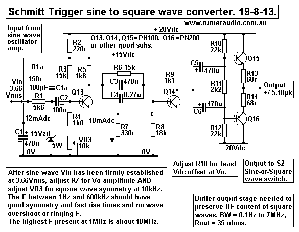
The input to the Q13 base network via the above R1 5k6 is
permanently
connected to the sine wave amp output in Fig 2, ie, output side of
R17, 33r.
The square wave converter works continuously while ever the whole
unit is
turned on, so that when switching from sine wave to square wave
there is
minimum delay while Vdc rails and working voltages establish
themselves
because long time constants are involved.
When switching S1 Fig 2 to sine wave, there is no sign of any
leakage of
square wave gate crashing the sine wave party.
As sine wave F rises above 500kHz, there are some difficulty
getting enough
energy to trigger the base input at Q13 and Q14 to maintain square
wave
symmetry.
To ensure enough triggering voltage at HF appears at Q9 base to
give symmetry,
R1a 150r and C1a 100pF have been added as a Zobel network across
R1 5k6.
This was found to have a negligible extra loading on the sine wave
amp at HF.
The Q15 and Q16 complementary pair emitter follower buffer
overcomes the
problem of attenuation of HF on positive going V rise at R9, 1k1.
The 1k1 is not a low enough resistance to overcome any stray C in
following
attenuator network, and the attenuator network has low minimum R
in of 770r,
so the buffer IS NEEDED.
The Fig 4 schematic has 470uF bypassing R6 15k. In most other
schematics
online, R6 is not bypassed, or bypassed with a small value of C,
perhaps 100pF.
But after trialling several values, I concluded 470uF was fine.
With no bypass C or low values of C, the delivery of positive FB
from Q9 collector
to Q10 base is rather too slow. And I found the square wave's
lower horizontal
had a large kink, so the wave looked wrong, and unacceptable.
The RC coupling as I have it works best.
VR3 and R7 must be adjusted carefully to get the wanted level of
+/- 5.17Vpk
AND good wave symmetry where both top and bottom horizontals of
the square
wave have equal length, and time between verticals is equal. The
range of VR3
pot movement needed to get square waves to occur at all is rather
small.
The R7 value was adjusted with a temporary pot to get the wanted
peak Vo while
VR3 was adjusted for best symmetry as R7 is adjusted.
Nobody else tells you that you MUST adjust these two resistors
together
because they are somewhat interactive, and beginners will be
frustrated when
they build something they saw online and it fails to work and they
stare at it for
10 years without knowing what questions to ask or what to try to
get it working.
When using 10kHz sine wave input you should get a splendid looking
square
wave and you should find all other F give the same peak Vo and
good symmetry.
I have no provision for applying DC offsets at the output, so that
in effect a
positive or negative bias voltage cannot be included in the total
Vo signal.
Nor can you vary the asymmetry for a weird looking square waves.
I have never needed Vdc offsets, and have always found that having
Vdc
content in signal gene outputs is a royal pain in the arse when
testing something
where you WANT ONLY 0Vac at the input to something you are
testing, and if
you do want some DC, then make up a suitable C+R coupling circuit
and add the
Vdc bias manually. If there is to be any biasing of amps under
test, it will be done
within the amp, which should not have any Vdc present at its
input, say from a
grid which is drawing some slight grid current at idle, and every
time you switch
sources you get a loud click.
I do not propose to add more boards for a "triangle wave" or saw
tooth wave, or
for AM or FM modulation. To test audio amps, there is no need for
more than what
this unit now does, ie, give sine and square waves up to 5.15Vpk
level, 1Hz to
1MHz, and with no Vdc content.
For the extra functions an additional box could be made with a
suitable circuit you
will have to research and develop after perhaps beginning with
something you'll find
online but which probably will not be fully explained properly, or
which just won't
work very well. A good triangle wave with straight lines can
indicate very basic
linearity of an amp because you can see when the straight lines
get a bend if you
have a dual trace CRO.
F distortion can occur, ie, "integration", ie, further action by
C&R or L&R circuits
within the tested amp. For measuring THD, it is better to use a
dedicated low THD
sine wave and following notch filter as described elsewhere at
this website,
thd-measurement.html
Because of long time constants used in the unit, Vdc settlement
after turn on
takes about 20 seconds before 0Vdc appears at the output with
negligible Vdc
measured. Some variation of the Vdc offset will occur with use and
switching F
ranges or from sine to square.
Vdc will eventually settle. Most good amps have a C&R high
pass filter at their
input such as say 0.33uF plus 68k, giving LF pole at 7.1Hz. The
time constant
= 0.022 seconds. This will cause serious distortion of LF square
waves. But you
will find the distortion where square wave horizontals become
highly sloped at
below 30Hz is of little concern. With this oscillator unit you can
place a bypass
link across the 0.33 uF and then the time constant is set by C24
200uF and 68k
plus R41 47k at unit Vo thus giving time constant of 5.5 seconds,
and LF pole at
input at 0.028Hz. The distortion of LF square waves is then
negligible.
At the unit's Vo, the R41 47k, gives a long time constant = 9.4
seconds when
unloaded. So where you have a tube amp with 0.22uF and 470k at
input, the
TC = 0.103 seconds, LF pole = 1.53Hz and you will still get square
wave distortion
at the input. If the 0.22uF was bypassed with say 22uF NP cap,
then you get a T
C = 10.3 seconds and square wave at input will keep its integrity.
However, tube amps have maybe 3 internal C&R couplings and at
least one R+L
OPT coupling which all cause trouble with square wave inputs. The
NFB used will
correct much of the errors in square waves that are inevitable.
But do the so called
errors with square waves at LF matter?
Fortunately, nobody has proved the C+R and R+L coupling causes bad
LF sound,
and in fact well made tube amps just cope, and sound is excellent.
What is important is the HF square wave performance of any amp and
its stability
with C loading or without any load at all.
The amp under test should be able to give a good looking
reproduction of square
waves between 100Hz and 5kHz.
There should be very little ringing or overshoot with no amp load
or with a pure R
load of nominal value +/- 100%.
So something designed for 8r0 should work OK with 4r0 or 16r0 even
though less
max Po is available.
Some overshoot may be allowed to occur with solely C loads between
0.05uF
and 10uF, and where Vo is kept low to avoid overload.
Many amps fail when tested with square waves and they can
oscillate badly at
some RF when no load is connected or when a pure C load is
connected.
Most dynamic speakers are inductive at HF and many do not have a
Zobel
network at their X-over filter to ensure there is a nominal R load
when F rises
above 20kHz, such as say 8r2 + 0.47u.
The beauty of square wave testing is that you can adjust the the C
value used
to bypass the FB resistance from amp output to its FB input port,
and adjust the
HF gain and phase change of the voltage amp to ensure HF gain at F
above
20kHz is reduced, along with phase shift so that FB remains
negative, and not
positive, even when C loads are used. A CRO and a good signal gene
are
essential tools for getting any amplifier to work well as it can,
and give optimal
bandwidth and complete unconditional stability when NFB is used.
In amps without NFB, the signal gene is still essential to make
sure sine wave
response is as wide as wanted. Without NFB, most amps have no
stability or
oscillation problems, but the CRO will tell you their transient
response is much
poorer than their brothers with well designed NFB networks.
Back To Education and DIY
Back to Index