TUBE
AMP POWER SUPPLIES.
Contents of this page includes:-
Definition of linear power supplies.
Fig 1. Basic wave forms for Vac and Iac in rectifier
circuits.
Earthing all devices for safety.
Mains Active, Neutral and Earth.
Basic operation of C, L in CLC filters.
Fig 2. PSU for 8585 amp, 2011.
List or all power supply requirements for a tube amp.
Discuss peak currents in diode rectifiers.
Fig 3. SHEET 3. 300W amp PSU chassis.
Fig 4. SHEET 4. 300W amp chassis.
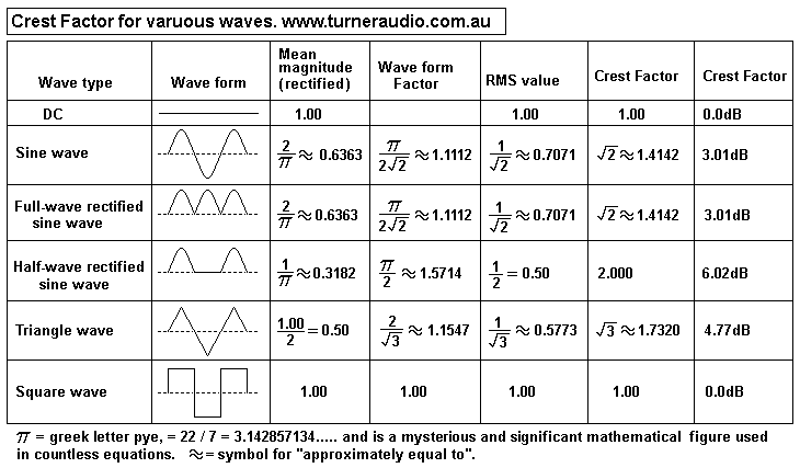
Fig 5. Crest Factors for various wave forms.
-----------------------------------------------------------------------
I had many questions about power supplies. "Power supply"
usually means a "linear"
type with mains power transformer, diode rectifiers, capacitors,
chokes, possibly
protection circuitry and regulators.
Linear power supplies are different to switch mode power
supplies, SMPS, which rectify
the incoming 50Hz or 60Hz mains frequency without a heavy mains
transformer. A single
electrolytic C is charged by diodes so that 240Vrms mains makes
+335Vdc. A solid state
circuit converts the stored energy to a HF square wave, usually
above 100kHz, and this is
fed to a very small HF transformer with ferrite core to make
square wave output that has
peak Vac equal to wanted Vdc.
Diodes charge small value C to make the wanted Vdc without any
50Hz ripple, and there
may be a small LC filter to remove the small amount of 200kHz
ripple.
SMPS are 1/20 of the weight and size of the traditional linear
types. They are routinely
used in all PCs and in many solid state amps.
AFAIK, no manufacturer has ever made a tube amp with a SMPS
power supply to give say
+450Vdc and say +6.3Vdc for B+ and for tube heaters.
In all tubed amplifiers, the mains Vac is applied across a
primary winding which has no
direct connection to several secondary windings which may
produce say 330Vac to make
+450Vdc, and 6.3Vac for output tube heaters, and 50Vac for a
-70Vdc bias winding.
Such simple linear PSU do not have any complex solid state
devices beyond silicon
diodes or some discrete transistors
for regulation.
Fig 1. Basic wave forms.
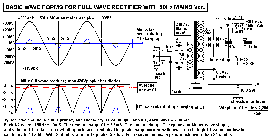
The waveforms in rectifier circuits rectifier should be
understood to avoid
excessive Vpk across diodes and excessive current peaks. I show
a brief schematic
for B+ where a 300Vac HT winding makes approximately +380Vdc at
160mAdc at
output of CLC filter.
The first issue is safety.
All power amps and preamps with PSU MUST have their chassis
connected directly
to the Earth connection at IEC socket.
The connection point should away from PT and to chassis near
input, with thick
green-yellow cable well bolted to chassis.
The 0V rail of the amp can be connected to chassis near input
using 10r0 x 5W.
This avoids noise between Earth and 0V rail getting to input of
amp.
For E+I power transformers, their yokes holding transformer and
or pot must be well
bolted to the chassis.
There are two wires coming into your house from the mains. One
is black, and called
the "Neutral" wire and is connected to ground at the house
circuit distribution board
via an earthing wire to copper water pipes or a copper clad
stake buried in the ground.
Vac between Earth and Neutral wires at amplifier is always a
very low Vac.
The Vac between Active mains wire and Neutral wire = 240Vac in
Australia
( or other Vac in your country ).
The Active Vac moves to +/- 340Vpeak as shown above and its
shape is often not a
perfect sine wave as shown, but has flat tops and bottom to
peaks because so many
people have devices connected which have rectifiers which cause
high peak currents
at near maximum peak Vac swings.
House wiring in Australia uses red for Active, black for
Neutral, green-yellow for Earth,
and white for switched wires. All appliances which require their
cases to be connected
to Earth directly can be accommodated such as washing machines,
but the energy
carrying circuit is via the red and black wires.
In the US the mains active is about 110Vrms, and has F = 60Hz.
The Vac wave shape of primary input is the virtually the same
within HT or any other
secondary winding.
The diode bridge switches the direction of current flow in HT
winding of each 1/2
wave of 50Hz so that the peak Vac is applied to C1. The output
Vac wave after diodes
is 100Hz with Vpk-pk = Vpk of HT winding, and it contains a lot
of 200Hz, 400Hz
harmonic content plus Vdc content. The C1 is thus charged up
with Vdc to nearly same
as the peak Vac in HT winding. Winding losses and diode
resistance cause the Vdc at C1
to always be less than the Vpk of HT winding.
Without any Idc flow, C1 will charge up to within 2Vpk of HT
Vpk. So for a 300Vac winding,
expect +420Vdc with no Idc load but when Idc flows, Vdc sags,
and HT Vac also sags.
The non loaded ratio of Vdc : Vrms at HT = 1.4, but with Idc
loading it may be 1.35 or
much lower especially if vacuum diodes are used.
With no Idc flow, C1 and C2 have the same Vdc and there is no
ripple Vac.
The diodes conduct for a small % of each 50Hz 1/2 wave. With
0.16Adc, I show
conduction time = 2.3mS for each 1/2 wave of 10mS. For the Vdc
to remain at a stable
level, the power flowing out of C1 for 10mS must be equal to the
power flowing in for
2.3mS. Thus it becomes obvious that when diodes conduct, their
Ipk must be higher
than Idc flow, and average Idc flow in diodes = 10 / 2.3 x
0.16Adc = 0.696A and the
peak charge idc = average charge current / 0.63 = 0.67A / 0.63 =
1.1Apk.
So the peak charge current can be much more than the Idc flow.
But it is reduced
by winding resistance losses.
There is Vac at C1 which will look like a saw tooth wave on CRO
when examined.
You will usually see the V wave during C charge being steeper
and lasting less time than
the V wave when no charge is occurring and Idc is lowering Vdc
at a rate governed by the
time constant behavior of C1 and the amp input resistance. The
time constant here is
governed by R = B+ / Idc = +380V / 0.16A = 2,375r, and
C1 value.
Time constant in S = CuF x R / 1,000,000 = ( 47uF x 2,375r ) /
1,000,000 = 0.111Secs
= 111mS. With no charging continuing, if Idc were to remain
constant, Vdc falls at a
constant rate to 0V in 111mS.
The amount of Vdc drop for 7.7mS = 380V x 7.7mS / 111mS = 26.4V,
and this equals
the Vpk-pk for ripple and each 1/2 wave of ripple = 13.2Vpk.
Because there is triangular wave, the Vrms value for Vripple =
0.577 x Vpk =
13.2Vpk x 0.577 = 7.6Vrms.
A simpler way of working out Vripple for 50Hz is Vr = Idc x
2,200 / CuF
and this case Vr = 0.16Adc x 2,200 / 47uF = 7.5Vrms. The Vpk-pk
ripple = 3.4 x Vrms
= 25.8Vpk-pk which agrees with basic time constant calcs.
Fot the formula Vr = Idc x 2,200 / CuF to be correct,
the Idc load > 20 x Xc.
The L1 + C2 act as second order low pass LC filter.
They have Fo pole = 5,035 / sq.rt ( L in mH x C in uF )
= 5,035 / sq.rt ( 4,000mH x 470uF ) = 3.67Hz.
At this F, L1 and C2 form a series resonant network which is not
damped by low
enough R to prevent LF resonance which tends to favor noise
between 2Hz and 6Hz.
However, this is well below AF band and causes no trouble.
The 100Hz attenuation factor = Xc / XL at 100Hz.
Xc = 159,000 / ( Cuf x F ) = 159,000 / ( 470uF x 100Hz ) =
3.38r.
XL = L in H x 2 x pye x F Hz = 4H x 6.28 x 100Hz =
2,512r, so
Attenuation factor = 3.38r / 2,512r = 0.00134, so Vr at CLC
output is reduced to 7.6Vrms
x 0.00134 = 0.01Vrms, and this is not going to create any
audible intermodulation
harmonics in amp output.
The typical noise at C2 is mainly all below 10Hz, but typical
total can be 50mVrms,
not large enough to cause audible distortion at amp Vo.
When silicon diodes were invented, bridge rectifiers and voltage
doubler arrangements
which are shown in textbooks were rapidly adopted to replace
vacuum diodes because
they offered much greater efficiency, lower cost and far better
Vdc regulation with change
of Idc due to their low "on" resistance.
Tube rectifiers have considerable series resistance often above
50r when conducting
current and thus dissipate heat from their anodes and they need
power to heat their
cathodes. So tube rectifiers help make the chassis hot, but do
nothing to improve the
music.
There are strict limitations on the C value being charged by
tube diodes because
allowable peak charge currents are typically less than 250mA.
Exceeding this value with C1 being too high causes internal
arcing and rapid tube
diode failure. But a single 1N5408 has rating for 3A continuous,
R on < 1r0, and
peak Idc can be higher than 3A.
With Si diodes, C1 could be 1,000uF, but there is no need. Use
of 220uF is OK,
and Vr at C1 = 1.6Vrms. But peak charge current is increased.
But it is limited by the
winding resistances, and 1N5408 has high enough current rating
to handle 1,000uF,
even at turn on when very high peak charge currents flow to get
Vdc high within 1
second after turn on.
The high peak charge currents with Si diodes and high C values
could cause problems
with noise if the earth path is not correctly done.
The wires between diode cathodes and + terminal of C1 and
between diode anodes
and - terminal of C1 should be short, but not include any length
along the 0V rail which
usually is a 2mm dia copper wire about 300mm long between PSU
and amp input.
Half wave rectifiers can be used where there is not high Idc and
Vripple does not
matter much.
The 1/2 wave rectifier may have the same Vac at the 300Vac
winding shown, but
one end is taken to negative terminal of C1, with other end
feeding C1 through
1N5408 to positive terminal of C1.
Vr for half wave rectifier = Idc x 4,400 / Cuf, so in
this case, Vr = 15.2V at C1.
The attenuation factor of L1 + C2 = 6.76r / 1,256r = 0.0054. So
for the same CLC,
50Hz Vripple at C2 = 0.081Vrms, which is 8 times higher than
with full wave rectifier.
All electrolytics must have high enough ripple current rating
and Vdc rating.
Ripple current = Vac / XC at 100Hz. For C1 = 47uF, and Vr
= 7.6Vrms,
Ir = 7.6V / 33.8r = 0.22Arms, and most 47uF x 450V now made have
much higher Ir
rating because they are designed for SMPS where Idc may be much
higher than for
a tube amp channel here which might supply 2 x KT88 plus its
input tubes.
Vdc may be +390Vdc when Idc flows. But with no Idc, Vdc may rise
to +420Vdc.
Thus C1 and C2 must be rated for at least +450V. If tube diodes
were used, to get
+380Vdc with Idc, the HT winding would have to be about 340Vac,
and with no Idc
the Vdc could soar to +480Vdc, and the 450Vdc caps may arc
internally and fail to
become a short circuit.
Where Vdc is expected to be high without normal Idc flow, use
470uF x 350V in series
with R divider to ensure equal Vdc is across both C. The high
Vdc can occur after
turn on before power tubes warm up after 15 seconds. With 5U4
vacuum diodes
which have directly heated cathode their warm up time is 2
seconds, so B+ can go
much higher than the normal working value before theIdc flow in
tubes reduces the
B+. So an amp with CT HT sec = 350V-0-350V and 5U4 will make B+
= +490Vdc
but when output tubes conduct the B+ falls to +410Vdc, so Vdc to
Vac conversion
factor = 410Vdc / 350Vac = 1.17.
The design of the power supply isn't difficult if we follow a
path through a series of
equations. I will base my mathematical processes upon an example
of a power
supply for the 8585 amplifier :-
Fig 2. 8585 amp, latest version 2011.
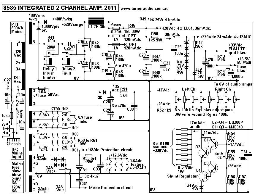
The above looks extremely complex, but it just uses repetition
of a few basic simple ideas.
The principles in the explanation of the above can be applied to
any other tube amp supply.
B+ plate supply.
The 8585 had two channels each with 4 x 6550 / KT88 / KT90, plus
total of 4 x EL84, and
4 x 12AU7 input tubes.
Power needed for each function = Iac x Vac at output of Sec
windings,
of Idc x Vdc at output of diode rectifiers.
Idc at B+ needed :-
Anodes KT90, 2 x 4 x 30mAdc = 240mAdc at idle.
At 100W continuous, both channels, max Idc = 720mAdc.
Screens KT90, ( 2 x 4 x 2.2mAdc ) + ( Idc in shunt regulator ) =
41mAdc.
Anodes EL84, 4 x 9mAdc = 36mAdc.
Anodes 12AU7, 4 x 6mAdc + plus shunt regulation 6mAdc = 30mAdc.
Miscellaneous other = 5mAdc.
Total maximum B+ Idc = 672mAdc = 832mAdc.
The max B+ power = 0.832A x 480Vdc = 399W.
If the HT winding is designed for 400W the winding will remain
cool for most operation
where total Idc power = 352mAdc x 480Vdc = 169W.
Losses in Si diodes may be neglected, < 3W.
Heater power needed :-
KT90, 8 x 6.3Vac x 1.8A = 90.72W.
EL84, 4 x 6.3Vac x 0.8A = 20.16W.
12AU7, 4 x 6.3V x 0.15A = 3.8W.
Losses = 5W, including in Idc rectifier for 12AU7 heaters.
Total heater power = 120W.
Bias Vdc for 8 x adjust pots for fixed bias = 135Vdc x 0.017A =
2.3W.
Total maximum power to amp from all Secondary windings of PT
= 399W + 120W + 2.3W = 521W.
Maximum power input to PT = 444.4W plus winding losses of 5%,
and core losses of 2% = 558W.
Va rating for PT = 600VA or higher.
The 8585 toroidal power transformer was originally 800VA rated.
I was originally
made by Harbuch in Sydney but it hummed badly with 240Vac at
primary without a
load so I estimated the turns per volt were too low and Bac was
far too high.
I removed the Secs, and added 33% more primary turns of same
sized wire for Bac < 0.9T.
Then I added a sec winding for 180Vac HT winding for B+ doubler
rectifier, and added heater
windings. The noise was much reduced to just low enough when
mounted in a sheet steel
box between the two OPTs also in steel boxes.
The Primary winding resistance increased 33% but was still
sufficiently low.
Altering this toroidal PT used up 2 days using a small shuttle
of about 1 turn in length, made
from a wooden dowel 22mm dia, with cut outs on each end on which
to pre-wind the wire
used for new turns.
I found that all toroidal PT purchased at Jaycar or anywhere
else were too noisy to use in
any amp I built, so nearly all amps I made after 1996 had E+I
transformers which all ran silently.
I found cheap NOSS E+I was OK but the Bac should never exceed
0.8Tesla, and then they
ran silently without getting hot from core losses. Core stack
height for NOSS must be 50%
higher than the same PT using GOSS E+I lams where Bac could be
1.2T.
The 8585 has a voltage doubler B+ supply because the HT winding
for a doubler rectifier needs
1/2 the turns of the winding needed for a bridge, and 1/4 of the
turns needed for a HT winding
with CT.
The doubler is in fact two half wave rectifiers in series, so
the 180Vrms charges C16 with
positive going waves and C17 with negative going waves.
The resulting Vripple is 100Hz, and no larger than use of a
bridge for same dc power.
Si diodes are 6A rated x 1,000PIV rated.
The efficiency of the doubler with Si diodes is very good. The
ratio of Vdc : Vac = about 2.65 for
working circuits with doublers, so HT Secondary Vrms = Vdc /
2.65 = 480V / 2.65 = 181Vrms.
The DC RL is lowest for maximum AB Po = Vdc B+ / Idc max =
480Vdc / 0.832A = 577r.
Most of the time the Idc to KT90 anodes is low so RLdc at idle =
480V / 0.352Adc = 1,364r.
I used a CLC filter to reduce Vripple at top of C18+C19 to very
low level. The choke is large,
with Rw < 30r, so Vdc drop across choke at idle < 11Vdc.
There is no active regulation to keep Vdc constant at C18, and
it is not needed. The slightly
continuous change of mains levels creates a constantly changing
Vdc level which creates
very low frequency noise and C18 with spectrum between 0.0Hz and
10Hz, with average
amplitude of +/- 50mVpk when most other people connected to the
mains are busiest in their
homes.
This VLF occurs in all amplifiers without active regulators and
it causes ZERO audible artefacts.
The PP output stages of tube amps have naturally good common
mode rejection of B+ rail
noise which appears at their OPT CT.
The noise appears and each end of OPT primary, and little
appears across the OPT primary,
so virtually none in transformed to appear at the secondary.
Calculation of C16+C17. I have 2 x 470uF in series for 235uF. Xc
= 6r8, and the minimum
DC load = 577r. Ratio of Load : Xc = 577r / 6r8 = 85 = OK at
highest Idc.
So Vr at C16 = 0.832dc x 2,200 / 235uF = 7.8Vrms max.
100Hz Iac in 235uF = Vrms / Xc = 7.8V / 6r8 = 1.15Arms.
Chosen C16+C17 have ripple current rating of several amps.
The maximum dc power at C16 = 480V x 0.832A = 400W.
The power from HT secondary = 400W + 2% Rw loss = 408W, and with
HT 180Vac,
Iac = 408W / 180V = 2.27Arms. Each 50Hz 1/2 wave is 10mS.
If the charge time is 2.5mS, average charge Iac = 2.27Arms x
10mS / 2.5mS = 9.08A and
peak Iac for charging C = 9.08 / 0.63 = 14.4Apk.
I found the 2 diodes with 6A rating and 1,000Vpiv were fine,
because 180V x 6A gives 1,080W.
The peak rating for Si diodes is much higher than the steady
state condition.
The temperature rise for the Si diodes is less than +30C so you
can hold a finger on the plastic
body and not get a burn.
But peak charge currents in HT winding are highest in the second
after turn on where the
Vdc in C16+C17 has to rise from 0V to +480V in a few wave
cycles.
In Fig 2 I show R41 100r 20W in series with with HT winding. At
turn on from cold, the 100r
limits inrush currents to more than 2.5Apk and after a second or
two B+ will reach 70% of
max and after 4 seconds, R41 is shunted by Relay 1, and peak
charge currents are not much
higher than 3Apk and B+ then reaches max unload value of +508Vdc
with reducing charge
currents. The tube heaters have 1/2 their hot resistance when
cold so at turn on the mains
winding has high inrush current to warm the cathodes but peak
Iac is not as high as the
charge Iac to C.
Tube cathodes begin emitting after about 20 seconds and reach
nearly full emission in 60
seconds.
If the amp is turned off, and on again after say 2 seconds and
all cathodes remain hot,
the delay circuit always works to reduce input charge current to
C16,17,18,19, 470uF.
With limited inrush current , mains fuse can be 3A slow blow, a
lot less than 6A slow blow
without limiting. The 3A fuse means input power can be 3A x
240Vac = 720VA, and fuse
would blow at about 850VA.
The mains fuse would only ever blow if the HT sec has a short
circuit, if two of the series
electro caps become a short, or if the OPT primary shorts to a
secondary winding.
There are 8A fuse links soldered in to each 6.3Vac phase of two
x 12.6Vac heater windings
for 8 x KT90 and 4 x EL84, so that a short in heater circuit
will blow a fuse.
There are 2 x 3A fuses on each 12.6Vac phase of two other
12.6Vac heater winding to make
12.6Vdc x 0.6Adc to 4 x 12AU7 preamp and input tubes.
The 50Vac bias winding has 1A fuse.
All these fuses will prevent having the "minor Sec" windings
fuse open or overheat.
But in some amps I have used a permanent series R between HT
winding and C, with typical
R value = 4 x Xc at 100Hz. So for a bridge of diodes charging
235uF, and with low winding
resistance of power transformer, using 27r x 10W resistance in
series with HT winding will
much reduce peak charge currents without causing a large
reduction of B+.
I have no such permanent R in 8585 but if there was one, it
would be say 15r x 10W between
terminal B of HT winding and R41.
The effect of the added series R is to make the charge time to
caps much longer, perhaps 4mS
for each 1/2 50Hz wave cycle lasting 10mS.
The 100Hz Vripple will become more like a triangular wave, less
like a sawtooth wave and
average charge current will be slightly more than twice the Idc
to B+.
In a class A amp, the slight reduction of B+ with the added
series R does not matter because
while the amp is in class A, there is no change to Idc and no
change to Vdc.
Some people are fanatics about capacitors. They say all PSU caps
should be polypropylene
with high Vdc ratings. I cannot share the zeal of fanatic
extremists because nobody I met during
18 years hand crafting amps for extremists, not one could ever
identify an amp which did not
have polypropylene filter caps and / or coupling caps. But I
always used the brand of caps they
asked for. They paid the higher price.
I have only ever used low value polypropylene well rated "motor
start capacitors" in a power
supply for a pair of 60W class A SE amps. The 1kW rated
transformer I wanted to use had a
HT winding with CT, 420V-0-420V, and would give +560Vdc at the
700mA required
for the two 60W class A channels. But I only wanted +470Vdc for
the cathode biased 6550
and did not want to have a hot running series resistance to
lower the B+ by 90Vdc which
meant resistor heat = 63W.
So I used series 6Amp x 1,000V rated Si diodes to charge a pair
of series 60uF x 450V rated
polypropylene motor start caps each about 52mm dia x 100mm long.
Effective input C = 30uF
to CLC filter. I used 22k across each C to equalize Vdc.
With Idc = 0.7A, 100Hz ripple = 53Vrms. The 30uF was followed by
a large 4H choke with
Rw = 20r which dissipated 10W. I then used 6 x 470uF x 350V
rated caps in series / parallel
for total of 705uF which gave Vripple of 50mV, quite OK for the
anode supply with CFB
arrangement of 12 x 6550 in the two channels. I then had
additional RC filtering to the
screen supply and input stages.
If ever the Idc was low at say 0.5Adc, the B+ would rise, and if
Idc was high at say 1Adc
the B+ would go low, and all 12 x 6550 had cathode biasing and
shunt regulated Eg2,
so the tubes would survive the change of Idc and B+ for any
reason.
For all power supplies, you must think about THE WAY SHIT
CAN HAPPEN, and install the
means to minimise the smoke production and the cost of following
repairs.
With input RCA sockets shorted to 0V, the 60W SE amps had noise
at the outputs < 0.25mV.
Although ripple voltage across the C1 30uF capacitor was high,
there is no dissipation in
the reactive elements of C or following L, and I got the V drop
I wanted without wasting
heat in a resistance. Pure class A amps don't need regulated
power supplies and their
B+ voltage can be allowed to drop if there is a fault and
without causing damage.
The 420V HT could have been used to make a choke input filter
with just LC, ie,
without the 30uF. The theoretical Vdc at output of LC = 0.88
x Vrms of Sec winding.
But this assumes the choke and HT winding has no resistance, and
Vdc is less than theory
suggests. But LC filters must have a bleeder resistance so that
without the load to tubes, the
bleeder resistance provides a load of 1/10 of maximum normal
load and then the Rw losses
of choke and HT winding is minimised.
The minimum L for choke = RL dc at minimum Idc / 900 for 50Hz
mains.
Thus if you expect perfect condition Vdc = 0.88 x 420Vrms =
369Vdc, and you have bleeder
Idc = 70mAdc, RL dc = 369Vdc / 0.07Adc = 5,271r, and L = 5,271 /
900 = 5.86H.
In the real world anything over 6H will do but if its Rw = 25r,
then with 0.77Adc the Vdc drop
is 19Vdc so you get 350Vdc, and the 3% Rw of PT will reduce this
to 340Vdc and if you want
cathode biasing with Ek at = +25Vdc, the Ea is +315Vdc and maybe
there is -10V drop on
OPT windings and Ea is down to +305Vdc, and for the 60W amps I
made this did not suit the
OPT primary load.
So LC input is a good idea but you MUST have the right Vac to
begin with. But a 6H choke
for 800mAdc is a real monster, maybe as big as the large heavy
OPTs I used.
I wanted Ea = +435Vdc, and an additional 35V for cathode
biasing.
Thus any amp with CLC which has B+ that is too high can have C1
cap value reduced so
the Vripple is high, peak charge currents are low, and B+ can be
varied by simply varying
the C value of C1. C2 can be as large as you like. The L must be
able to withstand Vac
without its core saturating with the high Vac ripple.
Rules for CRC filters.
Wherever you have a CRC or CRCRC input filter for B+, the total
R should not exceed
0.05 x RLdc.
Suppose your amp requires +400Vdc x 0.16Adc at OPT for 2 x KT88
with input tubes.
RLdc = 400V / 0.16A = 2,500r so total R should be 0.05 x 2,500r
= 125r max.
The DC power to 2,500r = 400V x 0.16A = 64W, and heat in 125r =
3.2W.
If CRC is used, and C1 = 470uF, then Vr at C1 = 0.16Adc x 2,200
/ 470uF = 0.75Vrms.
If the wanted C at OPT to 0V = 470uF, attenuation factor = XC at
100Hz / R = 3.4r / 125r
= 0.272 and the Vr at C2 = 0.0272 x 0.75Vrms = 0.02Vrms, not a
bad result.
Vdc drop across 125r = 20Vdc so Vdc at C1 = +420Vdc.
The Vr attenuation factor = 0.02Vrms / 0.75Vrms = 0.027, or 1 /
37.5.
The minimum attenuation factor for R+C section = 0.1.
2 x R+C sections would give factor = 0.01.
Now if you had CRCRC with 3 x 470uf, the R for both RC sections
may be 10 x XC
= 33r, and total R = 2 x 33r = 66r and vr at C3 = 0.75vrms / 100
= 0.0075Vrms which
is probably as good as anyone needs, and there is no problem
with resonance with L + C
below 20Hz. The choke need only be 0.54H but its Fo with 470uF =
10Hz, and this is
a bit high, so for 5Hz the L must be 2.2H for Fo = 5Hz.
Such a choke could have Rw 40r and for the expense of the choke
there is not a
huge benefit, especially for a PP amp with CMRR. But for SE amp,
the choke is best
for very low Vr = 0.002Vrms at OPT connection.
But consider CRCRC for 12 x 6550 for SE class A needing total B+
= 470Vdc x 800mAdc. RLdc = 589r. Total R should be 0.05 x 589r =
30r.
Heat in R = 19.2W. For two RC sections the R = 15r0 for each and
XC should be
15r0 / 10 = 1.5r, and required C3 at OPT to 0V = 159,000 / (
1.5r x 100Hz ) = 1,060uF.
You would us 10 x 470uF in series parallel for 1,175uF, and for
CRCRC you need
30 x 470uF x 350V rated. Vr at C1 = 1.5Vrms and at C2 Vr =
0.15Vrms, and at C3
Vr = 0.015Vrms. Vdc drop across 30r = 24Vdc . Total attenuation
factor = 0.01.
Now if you don't want so many C, you can use higher R value but
then the heat in R
increases.
This is where choke begins to make sense and for CLC you may
have C2 at OPT to
0V = 470uF with 4 x 470uF. If C1 = 470uF, Vr = 3.75Vrms, and if
Vr at C2 = 0.015Vrms,
the attenuation factor = 0.015V / 3.75V = 0.004, so XL = Xc /
atten factor = 3.4r / 0.004
= 850r and L might be 850r / ( 6.28 x 100Hz ) = 1.35H with Fo =
6.3Hz, probably OK,
and experience tells me it is not too hard to make a 4Kg choke
for 0.8Adc, L = 2H, and
Rw = 20r.
30 x 470uF at $15.00 each costs $450. 8 x 470uF cost $120, and a
choke might cost
$200, so CLC is cheaper than CRCRC.
For a preamp where Idc may never be more than say 60mAdc for 2
channels, then
CRCRC should be fine with 470uF and 100r so that 100Hz Vr at C1
= 0.28Vrms is
reduced to 0.00032Vrms at C3. The heat in 2 x 100r = 0.72W, and
quite acceptable,
with Vdc drop = 12Vdc, also OK.
For 8585 PSU, Choke L1 = 2H. I wound L1 with E&I T 25mm x S
40mm and filled
the bobbin with 0.55mm Cu dia wire. With correct air gap
material I got 2H at 0.6Adc.
XL at 100Hz = 6.28 x L x F = 6.28 x 2H x 100Hz = 1,256r. XC for
235uF at 100Hz = 6r8.
Attenuation factor = 6r8 / 1,256r = 0.0054, ( or about -46dB ).
At idle, with Idc = 320mAdc, Vr at C1 = 3.0Vrms, and at OPT
primary CT, Vr = 0.016Vrms
= low enough!
The Fo between L1 2H and following 235uF = 5,035 / sq.rt (
2,000mH x 235uF ) =
7.4Hz, a little high, but I found no strange behaviour occurred.
The amp DC Load = 480Vdc / 0.32A = 1,500r, and this is not low
enough to damp Fo
resonance for 2H + 235uF.
However, the 8 x 6550 or KT90 are all in parallel with each
having Ra at dc = 35k,
so with 8 tubes, dynamic resistance = 4k4 approx. The high Ra is
maintained by having
screen Vdc shunt regulated so Vdc between screens and cathodes
will not vary.
Triode connection of 6550 or KT90 will give each Ra = 1k1, so 8
tubes give 138r, and
this will damp the LF resonance because wanted damping R should
be 1.4 x XL or XC
at Fo. XC 235uF at 7.4Hz = 92r, and 137r is close enough to keep
the LC filter response
flat without a peak at 7.4Hz.
But because the CFB connection with regulated Eg2 is used, Ra is
high, but there is very
little change of Ia if the B+ wobbles up and down below 10Hz.
There is no change to
operating gm, and the B+ wobble is rejected by common rejection,
so the LF Fo resonance
of less than 100mVrms at around 7.4Hz just does not matter.
For SE amplifiers, low Vr at B+ connection at primary is
essential because there is no
common mode rejection. But where output tubes have CFB with
fixed Eg2, effective
Ra at very low F is quite high, and usually much higher than the
OPT primary load.
For ONE EL34 in pentode mode, its Ra at dc = 20k, but its anode
load = 5k0, so if
Vr at B+ = 20mVrms, it is divided over 25k, and the Vr across
load = 4mVrms.
If the OPT ZR = 5k0 : 5r0, then TR = 31.6 : 1, so Vr at sec =
4mV / 31.6 = 0.126mV.
But the CFB and GNFB will reduce this by about 1/10 or -20dB to
be 0.0126mV, well
below the other noise made by the amp.
Screen Vdc in 8585 and some of my other amps has been shunt
regulated by having
Idc to all screens fed through resistance to the B+. See
R49 3k6 in Fig2 above.
as the screen Idc input increases with output power, the Eg2 Vdc
tends to reduce and
cause the tubes to become under biased with less Idc at the zero
crossing point so THD
becomes worse. But some slight reduction of Eg2 is allowable and
as Ig2 increases a
shunt regulator reduces its Idc, so the Eg2 does decrease until
sustained high level Po
is maintained.
See Fig 2 above, with two series Darlington pairs
with MJE340 + BU208P.
If one or more 6550 or KT90 malfunction and Iadc goes high, then
Ig2 may go high, and
if high enough, the Vdc across the feed resistance R49 3k6 can
increase, and the regulated
Eg2 will be allowed to reduce, tending to turn off all tubes.
The shunt regulation shown
works well when music signals are taken up to clipping levels,
but without regulation,
Eg2 will reduce so much it causes high THD.
The shunt regulator is better than the series type regulator for
screens because the
series regulator does not allow the Eg2 to fall so easily if
there is a faulty tube where Idc
to its screen may increase from normal 3mAdc to 23mAdc, and the
tube overheats and
can cause trouble.
DC heater supplies for 8585 to 4 x 12AU7 give 12.6Vdc at 0.6A.
There is no need for CLC,
and I used CRC which worked fine.
There are more power supply schematics of working amplifiers
with PSU at my
listed web pages :-
300W mono blocs,
100W mono blocs,
5050 integrated,
SEUL 32W, 2012 version,
SE35W,
Quad II power amp mods,
Leak amp mods,
Dynaco ST70 mods,
10-tube preamp.
Chokes for CLC, LC are covered at my page powertranschokes.html
For a bench top PSU for testing tube circuits see power-supply-for-tube-tests.html
Fig 3. SHEET 3 Remote PSU on separate chassis for 300W
monobloc.
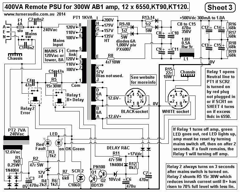
Fig 3 shows a 400VA PSU for 12 x 6550 tubes plus its input
stages.
Notice I have a voltage doubler rectifier for B+ which has 2
pairs of parallel diodes
each rated for 6A, but to maybe sure equal current flows I have
1r2 in series with
each diode.
At bottom left I have small PT2 7VA which turns on with large
mains PT1 1KVA.
PT2 makes +12Vdc to power a schematic which turns on Relay 1 at
3 seconds after
mains switch, so inrush current is halved because all mains
input current must flow
through R5 15r 30W.
Relay 2 turns on mains after PT2 is turned on by mains switch.
If umbilical cables
between PSU chassis and amp chassis are not properly connected
or there is a
fault in amp working with one of more 6550, or if PT1 is subject
to excessive Vac
input from mains, Vdc at output of R2 47r is pulled to 0V, and
Relay 1 is turned on
to interrupt the Neutral line to PT primary and red fault LED
glows, with green LED
turned off.
The owner must investigate why there is a problem.
A good example of a series type solid state regulator is here :-
Fig 4. SHEET 4. Part of power supply schematic on 300W
monobloc amp chassis.
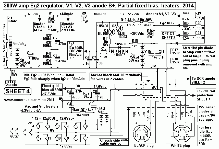
The series solid state regulator with MJ13003 and BU108 is for
screens for 12x 6550.
This regulator works to regulate for normal operation.
There was no way one faulty output tube could reduce the
regulated Vdc. But cathode
Idc of all tubes is monitored by active protection circuit so
that is one or more tubes conducts
too much Idc, the amp turns off automatically.
But if Eg2 output of regulator is shorted to 0V, then Vdc across
R11 10r0 increases and base
of Q2 is pulled down by 5 x 1N4007 series diodes so Idc is
limited to about 225mAdc, and
considerable Vdc is across R12+13+14 812r. The BJTs don't over
heat.
This is an interesting chart for Crest Factor for various wave
forms.
Fig 5. Crest Factors.
Back to Index Page