BENCH TOP POWER SUPPLY. 2018.
In 2018 I modified a bench top power supply I built in 2014.
The 2014 PSU replaced a more primitive PSU first built in 1995 and
which included 2 x 6080 in parallel
for tubed series regulator with a 6BX6 pentode for Vdc gain and
with a string of series 51V zener diodes
to be able to change output Vdc in +/- 51Vdc steps. I had switched
series R between B+ of +480Vdc
to 6080 anodes to reduce Ea of 6080 to avoid overheating. But I
found that while theory suggested my
regulator should have worked well for up to 250mAdc output, the
6080 arced internally and they became
unusable. 6080 and 6AS7 just DON'T LIKE excessive Ea and any
transient current peaks. I decided
to wave goodbye to my early PSU, I was sick of repairing it,
despite its circuit being exactly like in RDH4
and other respected circuits.
In 2014 I changed to a totally new schematic using high voltage
rated MJE34 for Vdc gain and 5 x BU208A
plastic pack bjts on a fan cooled heatsink. The series resistors
to limit Pd in Q were glued to a massive
sized plate using Selleys 401 silicone, and tied on with wire.
Years later, all R have survived well, silicone
is like new, and if you ever glue a white box ceramic R to bare
aluminium plate you have to break the R to
get it off the aluminium.
I had a couple of ganged rotary wafer switches given to me by
someone as junk, but unused NOS
mil-spec for serious currents, OK switching over 1Adc or 1Ac.
All the circuit items shown are surplus items left over after a
career as "amp worker" between 1994
and 2012 when I retired.
The circuit parts are screwed to 20mm thick slab of marine plywood
about 500mm wide x 500mm front
to back. All parts including heat sinks are covered by aluminium
cover from something made in 1980,
about 180mm high, and which I cannibalized for many useful parts.
So it is "breadboard construction".
I fitted a new metal front plate for fuses, output terminals, S1
Vdc select switch, and two -Vdc bias
adjust pots and LED indicators. There is a 150mm dia fan in rear
panel to fan air from rear towards
front past heatsink for bjts and past heatsink for series
resistors all mounted close to top cover.
Without any fan, the PSU could become very hot, but with a fan all
things remain cool.
But on a very hot day with 35C in my shed, the rise in temp caused
51Vdc zener diode voltage to
increase so that instead of say +534Vdc I got +540Vdc at output. I
am not aware of an affordable
Vdc reference device for 50Vdc steps which is immune to
temperature change.
I came up with this design...
Fig 1. 2014 Bench-top PSU.
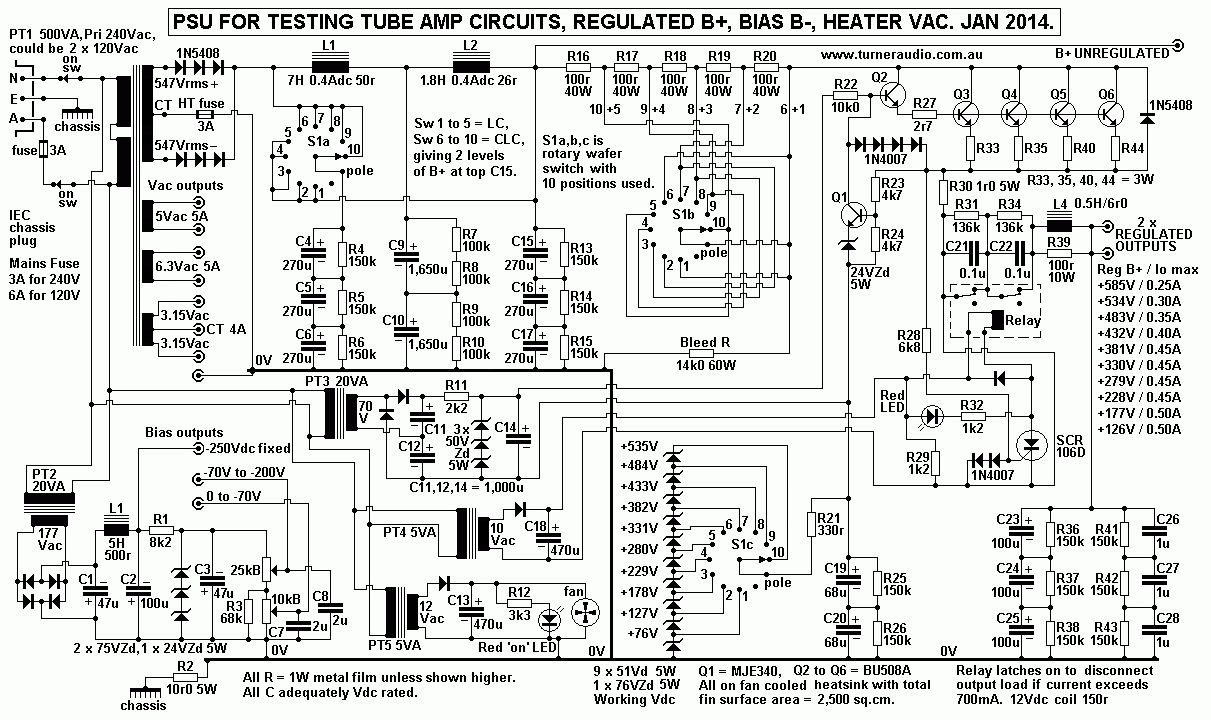
Fig 1 Schematic seems to work just fine and when using S1 to
switch the regulated B+ voltage upwards
or downwards between +126V and +586V with 51Vdc steps.
But while testing a pair of KT120 and other output tubes I found
the regulated 534Vdc output began to
sag the maximum Vdc input needed for 135W from the pair of tubes
with RLa-a about 2k2.
In Jan 2018 I wanted to repeat more tests with KT120 and other
tubes to give more detail to my edited
website page at loadmatch-5-beam-tetrodes-about.html
So I spent a couple of days improving the PSU, and here is the
latest schematic :-
Fig 2. 2018 Bench-top PSU.
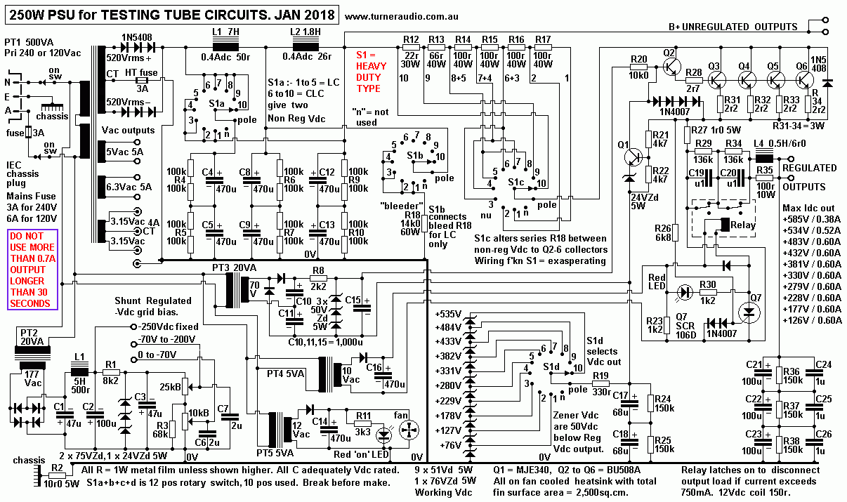
Fig 2 allows considerable increase in output current and on right
side I list the regulated Vdc with the
maximum Idc where regulation remains effective.
I can now get more than 500mAdc for all Vdc up to +534Vdc. Between
zero Idc for no load or 500Vdc,
typical Vdc sag is less than -3Vdc, due to the output having 7r0
in a small choke L4.
There are changes to PSU caps and series R values but it remains
reliable.
When 0.5Adc is generated, the Vdc at input to CLC filter is about
+587dc, so the PT1 plus diodes
is generating 587Vdc x 0.5Adc = 294W of B+ power.
PT1 was made in 1960s with unloaded HT winding having Vac
= 530V-0-530V where mains = 240Vrms.
So HT = +/- 749Vpk and with no load, Vdc at top C4+C5 = +745Vdc.
The core is T38mm x S96mmm. Afe = 3,647sq.mm, and Afe = 146.6 x
sq.rt Po.
Thus rating for max Pin = ( Afe / 146.6 ) squared = 24.87 squared
= 619W. For 240Vrms input, Primary
Iac = Po / Vac = 619W / 240V = 2.58A, so the RL at input = 240Vrms
/ 2.58Arms = 93r.
RwP loss = 100% x 3.5r / ( 93r + 3.5r ) = 3.62%.
The HT winding only conducts for 1/2 the 1,060Vac across whole
winding. Each 1/2 pri has 530Vrms
without any load, so TR = 530V / 240V = 2.208 : 1. Thus Sec Iac =
2.58Arms / 2.208 = 1.164Arms so
load = 530V / 1.164A = 455r. RwS = 63r, so RwS loss = 100% x 63 /
( 455r +63r ) = 12.16% so the total
loss for RwP+S = 3.62% + 12.16% = 15.78%, and to all this the core
losses may be 5% for all losses
= 20.78%.
The PT has an assumed capability for 5Vrms and 6.3Vrms secs giving
81W of Po, so that if winding
heater winding losses were 5%, 85W must be provided at input which
would reduce max input for HT
to 619W - 85W = 534W so that max Po at Sec = 534W = 20.8% =
422.9W, but only if the heaters
draw 81W.
The winding losses for HT windings in many old PTs were way too
high which led to many PTs in old
amps having fused HT windings when an output tube had bias failure
and its Idc increased hugely,
but the mains fuse did not blow.
This PT was not designed to make B+ with 0.5Adc continuously and
HT winding will overheat and fuse
open within 15 minutes.
When testing the PSU, I never had 0.5Adc for longer than 1 minute,
with Idc much less for next 5 minutes.
There was plenty of time to measure Vo at RL, Va, Vg1, and Eg2 and
Ig2 dc at high Po. The KT120
have Pda + Pdg2 exceeding all Pda ratings, but PT and and KT120
can withstand the abuse if it is NOT
continuous.
If you wanted to build this PSU then I suggest PT1 could have same
core VA rating for 620VA, but using
wasteless GOSS core T50mm x S72mm and window L75mm x H25mm, and
this window has 1.73 times
the area for T38mm core size so that larger wire sizes could be
used for all Vac and total Rw loss < 5%.
Instead of having 530V - 0 - 530V HT sec, it is better to have a
bridge with 530Vrms, and some would say
having a voltage doubler with HT winding = 265Vrms. (( I have
often preferred voltage doublers, and a
sample is at 300w-3+4-power-jan06_files/schem3-remote-PSU-400W-2014.gif
))
it is probably is easiest to have a bridge rectifier and 530Vac HT
winding could have 10 taps for
530V, 495V, 460V, 425V, 390V, 355V, 320V, 285V, 250V, 215V. This
gives Vdc with 0.5Adc load =
+660Vdc down to +268Vdc. If the choke for CLC was 50r, the same
series 100r x 50W can be used
between output of CLC and the SS regulator. This allows regulated
Vdc output from +585V to +126Vdc.
I have a separate floating 10Vac winding to power the overload
relay at output.
(( Instead, you could try a 1A circuit breaker in series with HT
winding, available from
https://au.rs-online.com
But they may work on peak Iac to charge C and may not like working
with Vdc at output. ))
I found the floating 12Vdc supply for output relay is 100%
reliable.
The PT could have bias winding, heater windings, and 10Vac for
relay supply.
--------------------------------------------------------------------------------------------------------------------------
For Fig 1 and Fig 2,
3 series 1N5408 are on each 1/2 of HT winding to give total PIV =
3,000V. Average diode current can
be continuous 3A with on resistance 0.8V / 3A = 0.27r, so diode
Pda can be 2.4W max, but working
average current is well below 3A. IN5408 can easily provide enough
current to blow the 3A fuse
between winding CT to 0V.
Before any fuse blows, I have Q7 SCR C106D which works a relay to
disconnect the PSU from
devices under tests if the Idc exceeds about 0.8Adc, which might
happen if the output is shorted or
a sudden high increase of Idc output occurs. I kept finding such
overloads occurred often during
testing and I fused a few BU208 in early versions of the
regulator. BU208 have 5A rating but if Vc-e
= 100V, collector heat = 500W, so they last for maybe 3 seconds
before needing a replacement.
I have 4 x BU208, so max heat could be 125W, so the device heats
more slowly, but there is time
for a fuse to blow, or for Q7 SCR to open a relay to interrupt the
excessive current surge.
The B+ filter elements of capacitors and chokes may be arranged to
form a capacitor input CLCLC
for highest range of Vdc from +585Vdc to +381Vdc.
The S1a allows C4+5 to be switched to be parallel to C12+13,
and filter becomes choke input LCLC
which lowers non regulated +Vdc to allow regulated Vdc between
+127Vdc and +330Vdc.
The switches S1a,b,c,d are in 4 rotary wafers of a very
heavy duty type. Each wafer has 12
terminals with one being the pole. 12 positions are possible with
1 position being where the pole
"points to itself".
In this application, I needed only 10 positions for 10 x Vdc
between 127Vdc at 585Vdc, in 51Vdc steps.
I did not want to let pole point to itself, or switch from +126Vdc
to +585Vdc, so the switch knob and
pointer have screw head stops on the front panel.
One terminal is not needed, marked "n", meaning nil, nothing, not
used.
There are two suitable screw heads to allow pointer to move to 10
positions only.
S1a moves C4+5 to C12+13. It changes CLCLC to LCLC
S1b connects bleeder R18 to top C4+5 so than even without
output load, there is about 35mAdc
load from which prevents non-regulated +Vdc at output soaring to
high Vdc, making Vc-e across Q2-Q6
too high.
All choke input type B+ PSU have some sort of bleeder R, see R18
14k.
(( It may be configured as a kind shunt regulator with 3 series HV
bjts, TO220 type, and a string of zener
diodes so that output Vdc is clamped to just above 0.63 x Vacpk
for HT winding. In LC mode, when Vdc
at C8+9 goes down with output current, the active bleeder shunt R
turns off, so you don't waste 35mAdc. ))
In my PSU, L1 is a massive potted 7H choke of 3.5Kg. I have 47r
10W + 0.33uF series R+C across choke
to maximise the L+C+R impedance at 100Hz which effectively makes
L1 act like it is more than 7H
and so less bleed Idc is needed to stop B+ soaring.
S1c varies the series R between non-regulated Vdc at top
C12 to collectors of Q2 to Q6.
When +585Vdc is selected, collectors connect directly to top C12,
but SCR prevents excessive Idc.
But for +127Vdc, there is a total of 288r between B+ of maybe
+400Vdc at C12 to collectors. +127Vdc
should remain regulated until Vc reduces to +128Vdc, so there is
272Vdc across 288r for 940mAdc.
Few will ever need 940mAdc at 127Vdc for a tube circuit. But the
LC input means peak diode currents are
far lower than for capacitor input so the HT winding has less
heating, according to Heat = Irms squared x R.
The PT1 may well have been originally designed for choke input to
give about +450Vdc which suits a very
large number of output tubes, and natural Vdc regulation is
better, and the low peak diode currents allow
tube rectifiers to survive far longer.
S1d selects the "reference Vdc" so that the Vdc at bottom
of 24V zener diode at Q1 emitter remains
at the zener diode selected by S1d.
R21+R22 both 4k7 form divider to drive Q1 base. Vdc across R22 is
nearly constant at 5.3mAdc.
Any tiny change of Vb-e at base makes a larger Q1 Vc-e change
which drives Q2 base, which spends
most of its time being at about 2Vdc above top or R21. Therefore
Vdc across R20 remains at a nearly
constant 123Vdc. Thus Q1 collector Idc = 12.3mAdc.
Total Idc flow to the string of 51V zener diodes = 5.3mAdc +
12.3mAdc = 17.6mAdc and thus heat in each
51V zener = 51Vdc x 17.6mAdc = 0.9W. The zener diodes are happy
with Pd < rating of 5W.
The whole Vdc gain circuit of R20 10k0, Q1, R22+R23 + 24V zener is
a simple single ended common
emitter gain stage powered by a floating Vdc rail of +150Vdc. PT3
has 240Vac mains input, and a 70Vac
sec and 2 voltage doubler diodes and C15 1,000uF acts just like a
150Vdc battery and so the gain of Q1
remains constant for whatever output Vdc is selected.
For testing an output tube, Ea may be between 100Vdc and 500Vdc. A
change of Ea = +/- 3Vdc makes
a negligible difference to tube operation and the idle Iadc and
biasing.
The L4 0.5H 6r0 plus C21 to C23 form low pass filter at output. HF
is prevented going out from regulator
and HF generated in any device under test is bypassed by C and
excluded from regulator with L4.
An increase of say +300mAdc L4 6r0 gives Vdc sag = -1.8Vdc, and is
negligible. An unregulated Vdc rail
may have 250r source R, so Vdc change = -75Vdc. Class AB testing
of output tubes requires stable
electrode Vdc.
There are 4 x 1N4007 to prevent Q2 to Q6 to ever be turned on
fully, so these Q are current limited.
R31 to R34 are each 2r2 which ensure Idc in each Q2 to Q2 remains
equal. Each 2r2 gives local negative
current feedback.
The output current from Q2-Q6 emitter resistors flows through R27
1r0 which is a current sensing R,
and if Vdc increases to about +0.88Vdc, it means Idc output =
880mAdc, and you have 0.88Vdc across
R26 6k8, which connects to Q7 SCR gate of C106d. it needs about
+0.68Vdc and 0.03mAdc to make SCR
latch on. With 0.03mA in 6k8, Vdc across 6k8 = 0.204Vdc, so if Idc
output exceeds about 850mAdc, the SCR
will latch on.
The SCR circuit and relay is supplied by +13Vdc rail generated by
small PT4 and half wave rectifier.
This 13Vdc rail has its negative side tied to bottom of R27. So it
acts independently. The SCR C106d latches
on it QUICKLY disconnects the regulator output from the output
load. But when Idc is interrupted in L4, there
is a back emf and could cause arcing across relay terminals.
To prevent arcing, C19 and C20 shunt the two sets of contacts
in DPDT type relay meant for switching
both active and neutral of 240V mains at 6A. Each relay section is
in series. If the Vo = +586Vdc, then
maximum Vdc across each set of opened contacts is 293Vdc, less
than the peak mains voltage rating of
340Vpk. I have never had any failures of the relays I use, 12Vdc
coil, Rw 150r, about 20mm x 25mm x 25mm
and easily sourced.
R29+R30 are 4 x 68k to divide the voltage equally across each pair
of open contacts.
To prevent excessive current surges when switching output +Vdc
upwards, L4 + C21-23 avoid fast switching
transients. However, having an L4 with switched currents means
there will be a back emf and I have R35 100r
to shunt L4 to keep its Z max < 100r. If ever the external load
being tested generates HF noise the 33uF shunts
it and there is at least 100r between load and BJTs.
Q2-Q6 are further protected to prevent the effects from some
voltage higher than the wanted output Vdc
causing reverse flow input current to emitters of bjts. Therefore
I have 1N5408 to to prevent emitter output Vdc
ever rising above collector Vdc by more than 0.7Vpk.
The Q3 to Q6 are in parallel and each with 2r2 current sharing R.
Their bases are paralleled, and driven by
emitter of Q2, and the Q2-Q6 forms a Darlington pair. The BU508a
has rather low Hfe because it is a high
voltage rated bjt so the Darlington connection is needed to
get the base input resistance of Q2 to be fairly high
to make a load which Q1 can easily drive.
To ensure that Q2 base voltage never rises too far above emitters,
there are 4 series 1N4007. I am not sure
of the final Hfe of the Darlington pair, perhaps about 100. This
means that if 0.4A is output current, Q2 base
input current = 4mA.
------------------------------------------------------------------------------------------------------------------
While testing KT120 in Jan 2018, I devised a screen Vdc reg for up
to 100mAdc and I suggest this may
be handy :-
Fig 3. Regulated B+ for up to +455Vdc at 100mAdc
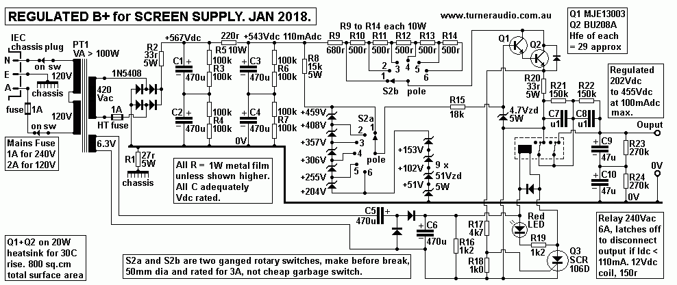
For Fig 1, I didn't bother using all nice neat switches and
protection relay but just re-soldered
wires and links to adjust zener diodes for wanted B+. The PT1 here
is well over 100VA rated.
Regulation is not quite as good as Fig 1+Fig 2 schematics for
anode B+ but will be good enough, ie,
Vdc won't sag more than 7Vdc. The data for BU208A is impressive
but Hfe minimum is quoted = 2.5,
but I found it was 29, and MJE13003 was also 29, so that if Idc
out = 100mA, then Idc in to Q1 base
= 0.12mA, so Vdc sag across R15 = 2.16Vdc, quite forgivable and
when there's a short to 0V, then R8
15k plus R15 18k have highest Idc = harmless 17mAdc. In this case,
Q1 and Q2 are fully turned on
with little Vc-e, so there's high Idc output which causes Q3 SCR
to latch on the open relay.
Notice the 0.1uF across the pairs of series relay contacts so that
you should not get an arc when
contacts open.
In my tests, when disconnecting a load from regulated anode B+, I
could easily generate maintain
an arc 10mm long between a lead with alligator clip to a number of
series wire wound resistances
which I assume must have a considerable inductance in series with
their resistance at HF.
People say you can get 150W with 2 x KT120 in Class AB1.
Almost nobody understands how to
achieve this. People say silly things to each other on the
Internet, and it is a wonderful place to view the
stupidity of ignorant fools leading ignorant fools. If you listen
to such idiocy and watch them rave you may
see clouds of smoke coming from the amps they make.
But I found that if I regulated both Ea and Eg2 = +500Vdc, you
could just squeeze 135W from a pair
of KT120.
If Eg2 is allowed to sag, you just cannot get the 135W. But Ig2 in
all beam tetrodes and pentodes rapidly
increases where Ea swings low, and Ia is high. So as high Po is
developed, screen Idc input much increases.
The increase if Ig2 can cause screens to have excessive Pdg2 and
screens can over heat, glow orange,
and the grid wires bend and become misaligned with grid 1 wires,
so tube is thus ruined.
Unfortunately, to get well above 100W from KT120, KT90, KT88 or
6550, the best method will have B+ up
to 700Vdc with Eg2 no more than +420Vdc, and I discuss all this at
loadmatch-5-beam-tetrodes-about.html
To build a regulated Vdc supply for +700Vdc takes more work. The
simplest way to regulate higher Vdc is to
use a massive PT with taps on a single HT winding for a bridge
with winding losses far lower than I used in my
above PSU. If you have idle Ea = +720Vdc, and it sags to +685Vdc
at max audio Po, then regulation is 5%,
and not too bad. But having +700Vdc at anode pin 3 in octal
sockets invites arcing to pin 2 for cathode heater
which is at 0V.
The higher Ea allows a lower Eg2 which should be regulated to
prevent the sag of Eg2 causing mis-biasing
because if Eg2 sagged -35V the Iadc is reduced by maybe 35mAdc, so
tubes act like they are operating in
pure class B, hence the crossover distortions.
I see little reason to ever try to make 150W from one pair of any
octal output tubes because it invites
overheating troubles, high THD, so it is always far more sensible
to keep Ea > +500Vdc, where 80W is easily
possible, and using 4 output tubes instead of 2 gives the 150W ppl
chat about, and with a considerable amount
of initial class A Po.
For testing tubes, having a series regulator as above is OK, but
in a real world amp the Eg2 should be shunt
regulated so that if Ig2 goes high, it allows the Eg2 to sag to
save the tube from overheating. Music signals
are similar to pink noise, and when pink noise is used for tests,
and when clipping is seen occasionally on wave
peaks the output audio Po may be 1/10 of maximum with a sine wave
with Vo from amp at -10dB below max
for sine wave. Then you find no need to be able to make high Po
with a continuous sine wave.
See my 8585 amp
page for details of the screen shunt reg supply.
For testing beam tetrode and pentode power tubes, I may use a
shunt regulator mounted on the test circuit for
the tubes, but all B+ power comes from the regulated B+ in above.
Besides the B+ filtering with L and C and the BJT regulator
element, I have put in a variable bias supply after
PT2 with -Vdc controlled by wire wound pots.
PT5 provides power for the fan with 24Vdc rated DC motor. But I
have applied only +16Vdc, and fan runs
slower, yet fast enough, but more reliably. The ON red LED is also
powered from PT5.
One might be tempted to make a shunt regulated anode supply. But
shunt regulation always involves having
high Idc flow in devices and R between the +Vdc rail and 0V. As
the devices under test consume more Idc,
the Idc in shunt regulator becomes lower, so Vdc sag can be
eliminated. But the PSU must work had all the
time and it makes everything stressed by heat. If 2 x KT120 in
class AB1 consume 400mAdc max, the shunt
regulator would need to have 400mAdc flow initially. Electricity
costs money, and heat eventually destroys
electronics. Where Idc is high, use series regulator say for
anodes, and maybe a shunt regulator for where
Idc is low, say for a screen supply.
Back to Education and DIY
directory
Back to Index page